


 Matric Group
1 min read
Why PCB Failures Happen: 6 Common Causes OEMs Can Prevent
Printed circuit boards (PCBs) are the backbone of nearly every electronic device. From industrial controls and medical equipment to defense systems...
1 min read
Printed circuit boards (PCBs) are the backbone of nearly every electronic device. From industrial controls and medical equipment to defense systems...
1 min read
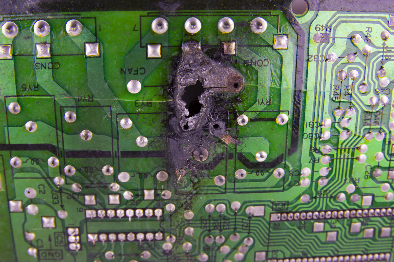
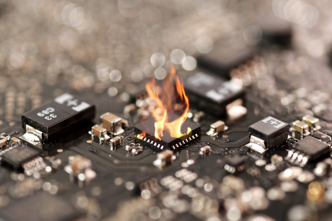
While there are many common printed circuit board defects, one of the most notorious is burnt components. It's also, unfortunately, one of the most...
1 min read
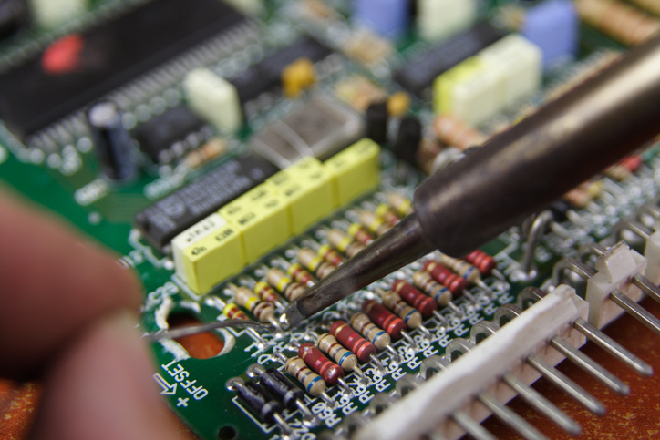
If you’re considering switching an existing electronic product design from through-hole technology to surface mount technology (SMT), you’ll want to...