1 min read
8 Steps to Electronic Product Design With Surface Mount Technology
If you’re considering switching an existing electronic product design from through-hole technology to surface mount technology (SMT), you’ll want to...

Printed circuit board (PCB) manufacturing is a process that requires precision and reliability.
As technology advances, laptops and smartphones are becoming smaller and yet capable of holding more data and completing complex tasks. This is thanks, in part, to the more efficient and complex PCBs available for installation in these devices - a result of the advances in production technology.
Finding the right partner that uses advanced Surface Mount Technology (SMT) will help to ensure your PCBs are project-ready upon delivery. Working with the right electronic contract manufacturer can mean the difference between receiving PCBs that are ready for installation versus a shipment of faulty boards that will delay production for your facility.
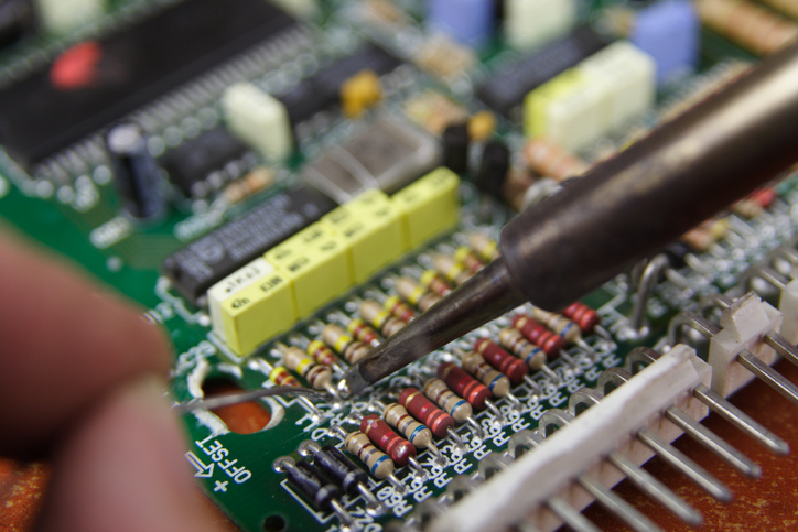
By definition, surface mount technology involves adhering components to the surface of the circuit board, rather than the older method of inserting leads through holes in the board.
Created in the 1960s, the SMT assembly process did not grow in popularity until the mid-1980s when the process was refined. By 1990, surface-mounted devices (SMDs) had become a popular integration. The SMT production process provides significant benefits that maximize first-run yield, including 
Another critical benefit of SMT production is its ability to allow for greater automation integration. This integration reduces production costs while increasing output.
SMT manufacturing also allows for much smaller components to be placed efficiently. Current processes allow for components as small as the 0201 package, which measures 0.25 mm x 0.125 mm. A four-machine line of chip shooters can place these components at a rate of 100,000 parts per hour. Each machine averages 25,000 components per hour.
The process is also more efficient as the components can be easily sorted and adhered to the board without concerns related to human error.
For further information on the inspection process for the SMT line, consider this free resource:
SMT involves several steps, from material preparation and the design phase to programming the machines to complete the task successfully and design implementation.
Components adhere to the board in two possible methods:
Next, components are placed over the paste, then reflow soldering occurs, followed by cleaning and inspection.
PCB manufacturing is a process that involves more than component adherence to the board. For a look at the capabilities Matric has for design, assembly, and testing, download this resource:
Due to the advanced nature of SMT lines, the setup process requires specific and strategic planning to optimize product flow. This meticulous planning results in more efficient product runs that flow at a reliable rate and ensure on-time order delivery.
The process includes:
Solder paste is fine solder particles that are suspended in flux. Commonly, the paste is identified as Type 3, Type 4, or Type 5. The type number indicates the size of the particles in the solder powder. The paste is carefully applied based on precise designs created through a computer software program. During the solder paste inspection, the volume and alignment are both evaluated for accuracy.
A slight misalignment could result in a defective board, while not enough or too much paste can interfere with the overall quality and lifespan of the product. It also evaluates any scratches or imperfections that occurred during the paste application.
Once the paste has been applied, the components for the PCB are then placed on the board by a pick-and-place machine. These machines can be placed in a series to improve throughput.
Next, the PCBs pass through an Automated Optical Inspection (AOI) station.
AOI is a visual inspection used to test for defects. This method works best for high-volume production environments.
Time-consuming and often complex, AOI requires hours of programming and involves the setup of a specific location inspection for the components of the PCB.
AOI is set up with narrow parameters to check for a particular design or part configuration. AOI PCB inspection is especially important after solder reflow.
This inspection method catches defects in parts placement or defective solder.
For SMT lines, the reflow oven melts the solder paste with a four-step process:

During this process, the components have permanently adhered to the board under optimal temperatures for setting the paste without damaging the components or compromising overall board quality.
The reflow is precise and saves production time.
Post-Reflow AOI is an inspection after the product completes its travel through the reflow oven. This inspection is set up to catch issues that have been identified in previous product runs, such as missing components or bad solder joints.
With both pre-reflow and post-reflow AOI, Matric has been able to improve the first-run yield from 70% to 97%.
Matric Limited relies on Surface Mount Technology for our PCB manufacturing process. The process provides reliability and has allowed Matric to address and resolve issues with first-run yield, as well as component orientation and location concerns during PCB production.
The SMT production process took almost 30 years to catch on. However, since then, popularity has grown, particularly to improve electronics size and efficiency. Working with the right partner can mean more reliable delivery time and better quality yield. Both of these can be attributed to the use of SMT production processes.
Are you looking for an electronics contract manufacturer with SMT production capabilities? If you are interested in learning more about Matric but can’t make it to our facility, we also offer virtual tours! Schedule your virtual or in-person tour today by clicking the link below!

1 min read
If you’re considering switching an existing electronic product design from through-hole technology to surface mount technology (SMT), you’ll want to...

1 min read
As today’s electronics designs become smaller and more complex, more engineers are relying on surface mount technology. After the 1980s, this...