1 min read
How to Tell Tombstone PCB Defects ‘Rest in Peace’
Working with small circuit board areas can increase the risk of various PCB defects, tombstoning in particular. While the grim nature of “tombstone”...

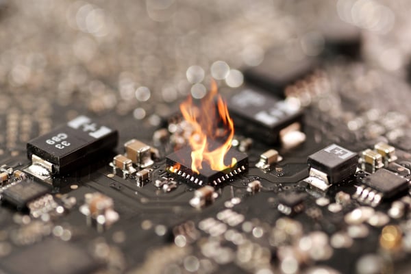
While there are many common printed circuit board defects, one of the most notorious is burnt components. It's also, unfortunately, one of the most damaging defects, as it can be difficult to repair and challenging to diagnose where the issue stemmed from.
In this post, we'll get to the bottom of what causes a circuit board to burn as well as how to fix it. Here's a closer look:
Before we get into PCB failure analysis techniques, let's first take a look at some of the reasons why a printed circuit board may burn. Burnt circuit boards aren’t necessarily a defect by themselves, and they are frequently caused by other inconsistencies or defects on the PCB.
Three of the main reasons PCBs end up burning are:
If PCBs are exposed to high temperatures, then it's only natural for this threat to become more likely.
However, most PCBs used in hazardous areas are built to withstand high temperatures and have a Tg (glass transition temperature) of 170°C. PCBs designed for hot environments must have an operating temperature 25°C less than the Tg.
But, accidents can happen. If a machine overheats or the board is exposed directly to flame, then that might not be the best situation for your components.
Most electronic parts do not work well above 70°C, so designing for high temperature applications is tricky, but necessary.
Another leading factor are situations when components are packed too close together on the printed circuit board.
Components that don’t have the necessary space on the PCB tend to heat up and could impact adjacent components that are more affected by high temperatures.
In other words, you want to avoid overstuffing the board. Not only will this reduce costs and accelerate production, but it can also help you avoid any costly mistakes that could come to bite you later down the road.
The most important part of manufacturing a PCB is the design phase, so if something is not quite right in the design phase, there will likely be consequences down the road. That being said, checking to make sure the right diodes and capacitors are specced out for the board will decrease the likelihood of component-failure related burning.
Boards might burn because of poor protections. The lack of properly sized fuse protection should be number one priority. A high voltage protection diode protects the board from burning in the event of a lightning strike or other voltage surges.
Other reasons for board burning are related to technician error. If the board connections are hooked up incorrectly or attached to the wrong type of power supply, leading to eventual burn out. In addition, if installation documents are confusing or nonexistent, a field technician might hook up the board improperly.
Conducting a PCB failure analysis is key to improving the product and preventing future defects from occurring. Here's a look at some questions that we suggest asking that can likely help you resolve burnt component defects:
Low quality parts are likely to have low quality outcomes. Preventing defects from occurring - whether it's now or in the future - can often be as simple as just ensuring proper component quality.
Always make sure to send your design to your board house for review before manufacturing -- think of it as a second pair of eyes on an email before you send. They may catch a mistake you missed.
While not a direct factor in what causes PCBs to burn, improper conformal coatings can negatively affect your PCBs. If dust or other particles make their way near already-hot components, they could ignite.
The four common coating types are brush, spray, dipping, and selective - and they all have their sweet spot when it comes to ideal use.
There are also different coating materials to consider, such as:
Make sure you know your coatings and which types of material would serve your PCB the best.
Circuit board overcrowding isn't just more likely to lead to burning, but to manufacturing challenges as well. Sometimes, preventing defects can be as simple as ensuring more adequate spacing on the PCB. Better spacing for high voltage and higher current traces can also decrease the risk of burning out a PCB.
In addition to spacing, ensure the PCB has the proper heat sinks and tracework. Your PCB might need a bigger copper layer depending on the application, so always double check.
While the designers and the manufacturers might know the best way to install a PCB, not everyone does. To avoid technician error-related failures, manufacturers can employ a couple of different methods to give the technicians the right information.
The first is installation documentation. This “manual”, so to speak, details the proper hook up information for each PCB.
Another method is a bit more intuitive, and it includes coding the types of connectors. Manufacturers often clearly label the PCB connectors with different colors or numbers and provide a key so the technician knows what goes where.
PCB defects like burnt components can be a real pain, but partnering with an electronic contract manufacturer who has experience with PCB assembly can make all the difference.
Check out our free sizing charts to help you keep your boards in ship shape!

1 min read
Working with small circuit board areas can increase the risk of various PCB defects, tombstoning in particular. While the grim nature of “tombstone”...

1 min read
At this point, we’re all familiar with light-emitting diode (LED) lights. From the bright, efficient bulbs replacing the old filament lamps, to the...

1 min read
Prototyping isn’t reserved for high-tech vehicles or revolutionary consumer gadgets. It’s also a great practice for manufacturing printed circuit...