


 Matric Group
1 min read
PCB Testing Methods: How to Test a PCB & Ensure Circuit Board Reliability
When you order printed circuit boards, you already understand the costly consequences of failure. The last thing you need is for your PCBs to...

Deciding on the best testing method for your printed circuit board can feel overwhelming. You’re balancing cost, coverage, and development time, all while trying to ensure your product performs reliably in the field.
Two of the most common PCB testing strategies are ICT testing and flying probe testing. Each offers strong defect detection, but the right choice depends on your production goals, design complexity, and timeline.
So, how do you decide which is the better automation test solution?
It starts with understanding how they compare and where each fits.
In-circuit testing (ICT) and flying probe testing (FPT) offer similar coverage in their tests, discovering most manufacturing defects that often occur in printed circuit boards (PCBs). These include:
The two, however, differ on their:
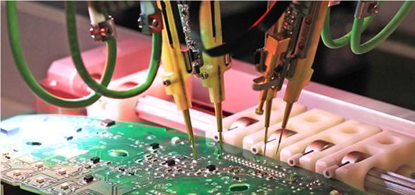
ICT is a powerful tool for PCB testing. It uses bed of nails in-circuit test gear to access the circuit nodes of a board and check the performance of each component. It can also test some functionality of digital circuits, although the complexity involved can make it economically prohibitive.
ICT is most suitable for testing products that are more developed and high-volume. However, the up-front costs and development lead time with ICT are higher and longer, respectively, than those of flying probe testing (FPT). This is because your manufacturer must explicitly create a custom ICT fixture for each PCB.
The good thing with ICT is that after the tool is developed, costs per unit tend to be lower than with FPT because it only takes about 1 minute for one test cycle. With FPT, it can take up to 15 minutes per board.
ICT is built for efficiency once it’s up and running.
Test cycles are fast, often around one minute per board. That speed drives lower per-unit costs at scale.
It also offers:
The trade-off is in setup.
ICT requires custom tooling and programming, which increases up-front costs and extends development timelines. It’s not ideal if your design is still evolving.
It also won’t test:
(Photo courtesy Doxals)
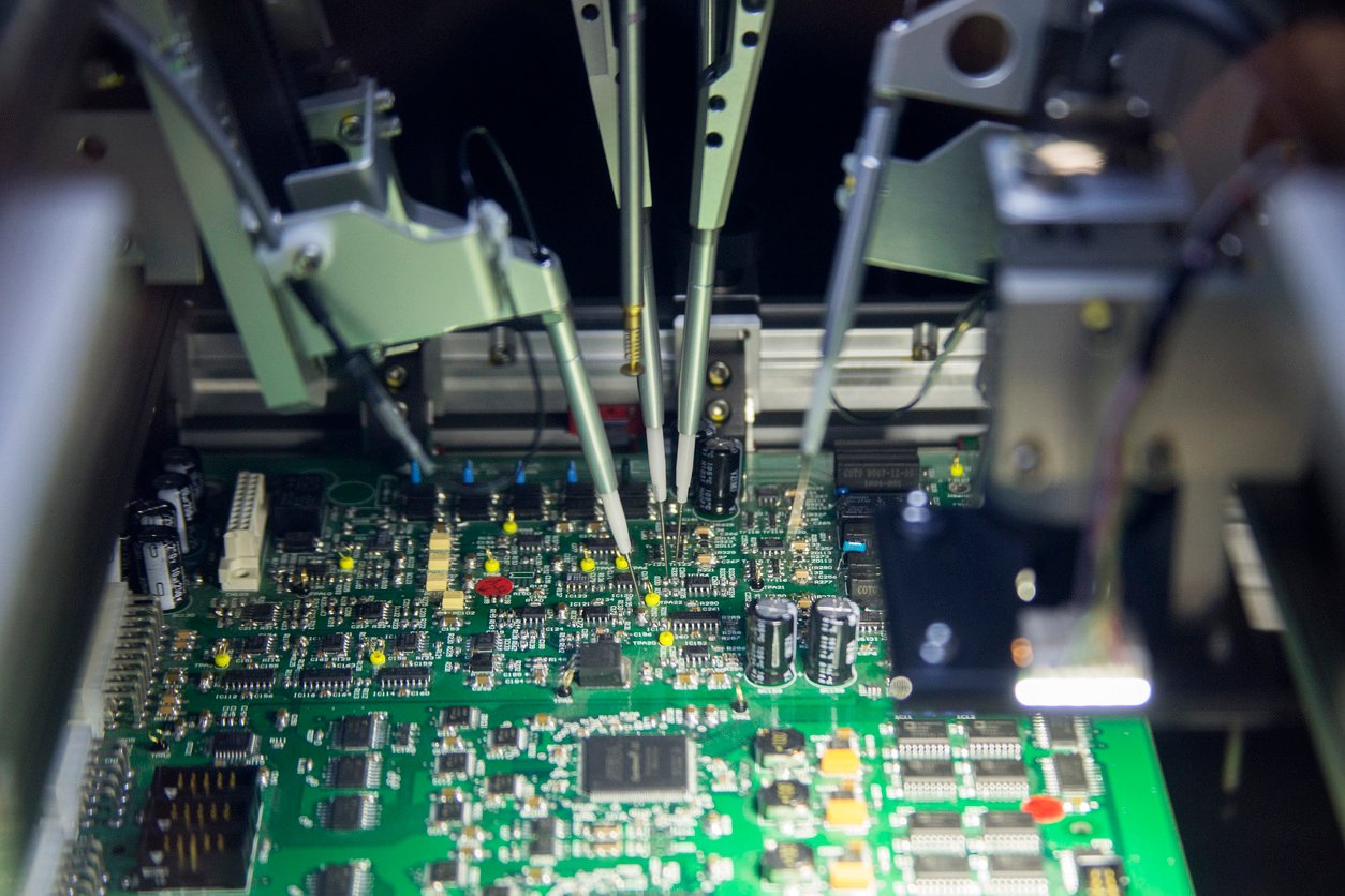
Unlike an ICT machine, an FPT does not utilize a bed of nails fixture. Instead, it uses a small number of movable and fixed probes to easily make a simultaneous in-circuit test of the top and bottom of your PCB. This can also be simply called a flying probe tester. It’s made up of high-precision needles -- some machines use as few as four needles, while others can use as many as 20 per PCB side. They’re programmed to contact component pins and perform electrical and functional tests to determine if the board is fit for the field.
FPT is most suitable for products that are in the early stages of development and are low-volume orders. It requires no custom tooling, and customization for each PCB is carried out through programming using the CAD data you provide to the manufacturer. With FPT, costs-per-unit are higher compared to ICT because of longer test cycle time periods per test system (up to 15 minutes).

FPT eliminates the need for custom tooling. That alone reduces both cost and lead time during development.
It’s driven by CAD data, so test programs can be created quickly and adjusted as your design changes.
Key advantages include:
The downside is speed.
Test cycles can take up to 15 minutes per board, which increases per-unit cost. That makes it less efficient for high-volume production.
Like ICT, it also doesn’t test:
All in all, the choice between ICT and FPT will depend on several important factors of your project. To recap, these include:
Remember to consult a well-rounded contract manufacturer for professional guidance. There may be other PCB testing and inspection options that are better suited to your design. Learn about those other options with our free guide to PCB testing!

1 min read
When you order printed circuit boards, you already understand the costly consequences of failure. The last thing you need is for your PCBs to...
1 min read
PCB design can be challenging. The complexity of your project and the potential consequences of PCB failure may require thorough, high-level...
1 min read
Tests for printed circuit boards (PCBs) come in many varieties based on cost, breadth, time, and other factors. There are many ways to test your...