


 Matric Group
1 min read
Why PCB Failures Happen: 6 Common Causes OEMs Can Prevent
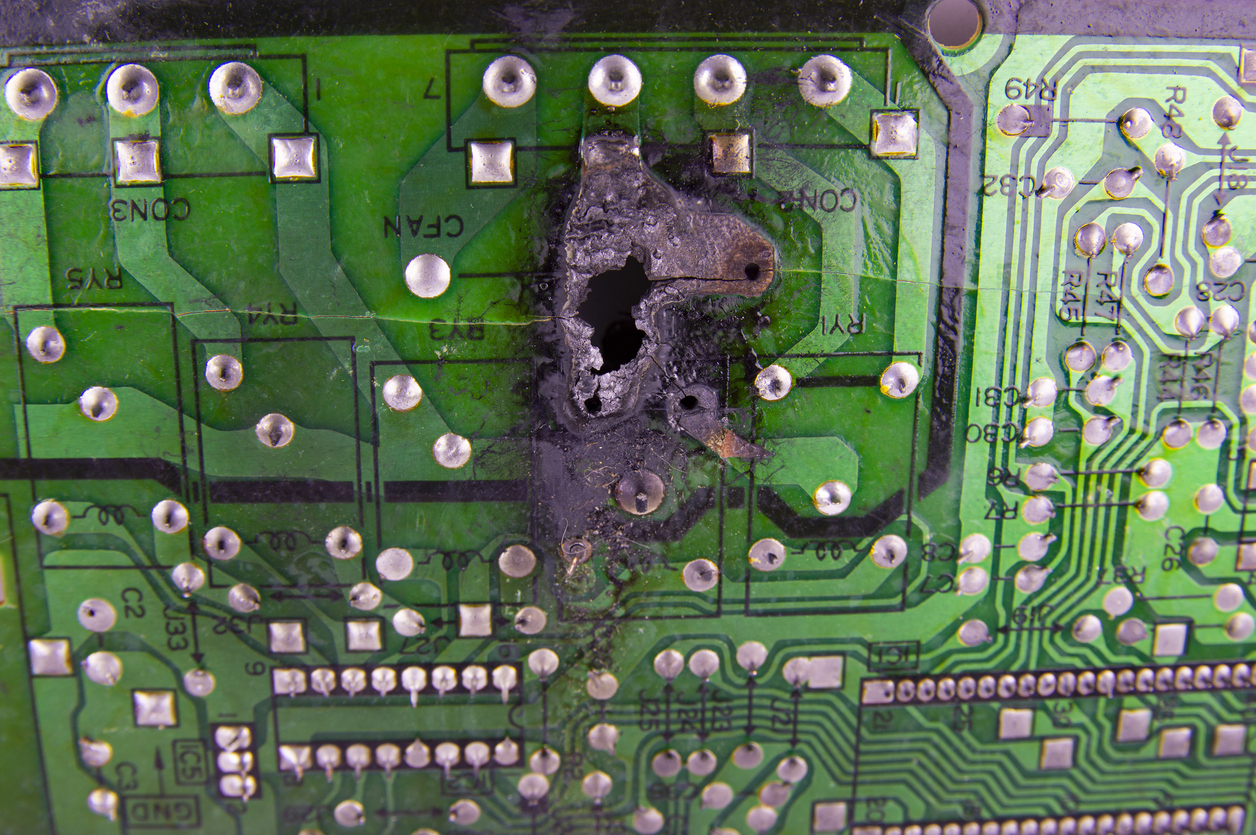
Printed circuit boards (PCBs) are the backbone of nearly every electronic device. From industrial controls and medical equipment to defense systems...

1 min read
Printed circuit boards (PCBs) are the backbone of nearly every electronic device. From industrial controls and medical equipment to defense systems...
1 min read
Working with small circuit board areas can increase the risk of various PCB defects, tombstoning in particular. While the grim nature of...
1 min read
There are many areas in life where accepting mistakes as inevitable is a good thing -- electronics manufacturing is not one of them. The end goal...