1 min read
What Are PCB Functional Testing Services?
Electronics manufacture and testing are like squabbling siblings. PCB testing is a necessary expense that, when done correctly, prevents much larger...
6 min read
 Matric Group
:
Feb 23, 2026

When you order printed circuit boards, you already understand the costly consequences of failure. The last thing you need is for your PCBs to suddenly fail or have a shortened lifespan because of a design or QA issue.
PCB assembly testing methods are a critical part of the manufacturing process. Reputable electronics contract manufacturers offer a variety of testing options, but the seven main types include:
Before we dive into each method, let’s first answer a common question.
If you’re wondering how to test a PCB or how to test a circuit board, the answer depends on your product, production volume, and reliability requirements.
There isn’t just one single test. PCB testing is typically a layered process that moves from basic inspection to full functional validation.
Here’s how it usually works.
Testing often starts with a visual review. This can be done manually or through automated optical inspection.
At this stage, manufacturers look for:
Catching visible issues early helps prevent larger production problems later.
Next comes electrical verification. This ensures the board matches the original design and that components are properly connected.
Common methods include:
These tests check for opens, shorts, resistance issues, and other electrical problems.
Once electrical integrity is confirmed, the board may be powered up.
Functional testing verifies that the PCB operates correctly in its intended environment. For high-reliability industries, additional stress testing such as burn-in testing may follow.
Testing a circuit board isn’t a single action. It’s a structured validation process designed to catch issues before your product reaches customers.
Now let’s take a closer look at the seven main PCB testing methods your ECM may recommend.
Before choosing a testing strategy, it’s important to understand what each method is designed to do. Some tests focus on electrical integrity, others verify functionality, and some are used to detect hidden structural defects.
In many cases, manufacturers use a combination of methods to achieve the right balance of cost, speed, and reliability. Below are the seven most common PCB testing methods and when they’re typically used.
In-circuit testing (ICT) is the most robust type of PCB testing in existence. The high price reflects that -- tens of thousands of dollars, though the cost will depend on board and fixture size, among other factors.
An ICT, also known as a bed-of-nails test, powers up and actuates the individual circuitry on the board. In most cases, the test is designed for 100% coverage, but you’ll get closer to 85-90% coverage. The nice thing about ICT is that the 85-90% you get is totally free of human error.
This test involves using fixed probes laid out in a way that matches the design of the PCB. The probes checks the integrity of the solder connection. The bed of nails tester simply pushes the board down on the bed of probes to start the test. There are access points predesigned in the board that allows the ICT testing probes to make connections with the circuit. They put a certain amount of pressure on the connection to make sure it stays intact.
ICT is often performed on bigger connections and ball grid arrays (BGAs).
This test is for a “mature” product with very few revisions expected. If you don’t have design-for-manufacturing as part of your goal, with the proper pads on the board, you may not be able to use an in-circuit test. Unfortunately, you can’t change your mind and move to an ICT strategy halfway through production.
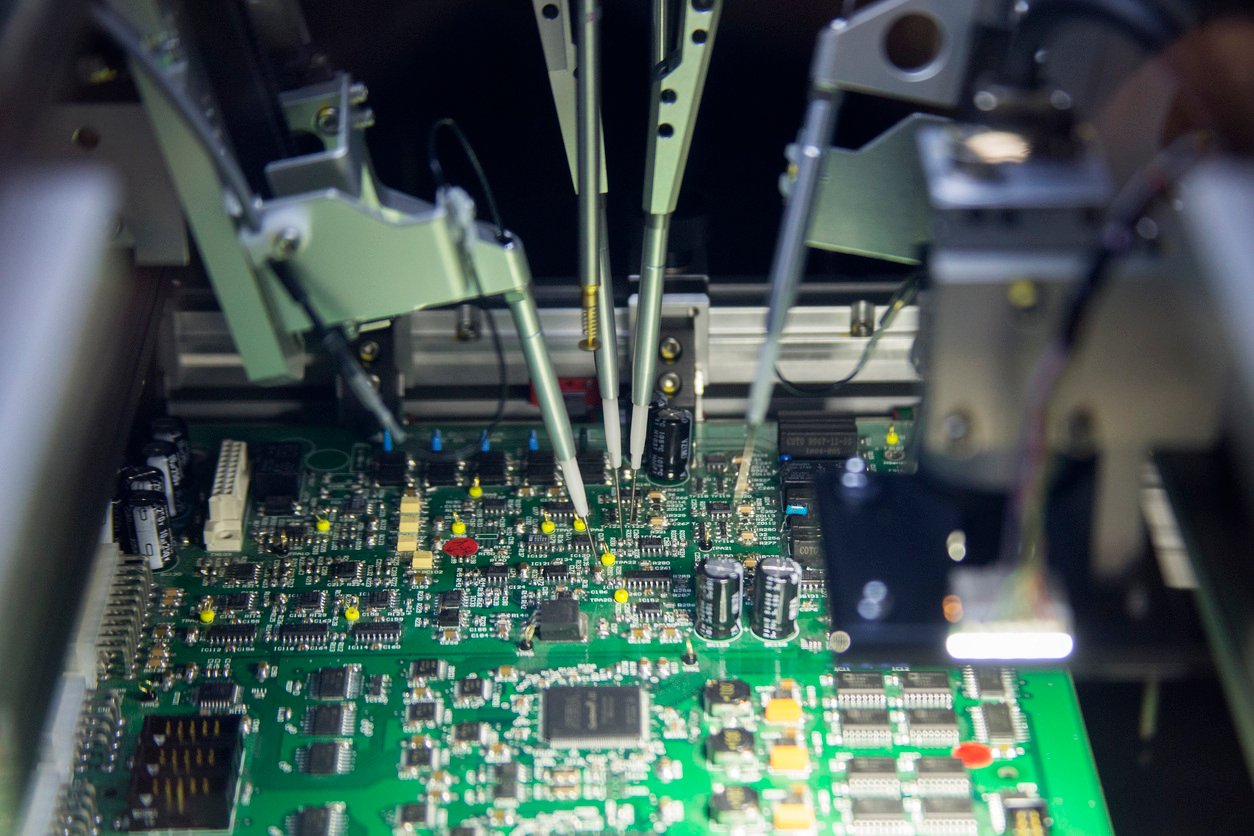
Flying probe testing is a tried-and-true option that’s less expensive than in-circuit testing. It’s a nonpowered type of test that checks for:
The flying probe tester works through the use of needles attached to a probe on an x-y grid obtained from basic CAD. Your ECM programs coordinates to match the circuit board and then runs the program, connected to those test points.
We touched on flying probe vs. ICT being a common comparison. Each has advantages and disadvantages.
In some cases, ICT makes it unnecessary to use flying probe testing, but the PCB has to be designed to fit with the test fixture -- which means a higher initial cost. ICT can be faster and less error-prone than flying probe testing, so you might find the extra cost is worth it. While flying probe testing can be cheaper initially, it may actually be less cost-effective for large orders.
One final word of caution: A PCB flying probe test does not power up the board.
Have questions about our design, assembly, or testing capabilities?
Download our free guide below:
AOI uses either a single 2D camera or two 3D cameras to take photos of the PCB. The program then compares the photos of your board to a detailed schematic. If there is a board that does not match the schematic to a certain degree, the board is flagged for inspection by a technician.
AOI can be useful for detecting issues early to ensure production is shut down ASAP. However, it does not power up the board and may not have 100% coverage for all part types.
Never rely solely on an automated optical inspection. AOI should be used in conjunction with another test. Some of our favorite combos are:
As the name suggests, burn-in testing is a more intense type of testing for PCBs. It’s designed to detect early failures and establish load capacity. Because of its intensity, burn-in testing can be destructive to the parts being tested.
Burn-in testing pushes power through your electronics, usually at its maximum-specified capacity. The power is run through the board continuously for 48 to 168 hours. If a board fails, it is known as an infant mortality. For military or medical applications, boards with high infant mortality are clearly not ideal.
Burn-in testing isn’t for every project, but there are some cases where it makes a lot of sense. It can prevent embarrassing or dangerous product launches before they reach customers.
Just remember that burn-in testing can shorten the product’s lifespan, especially if the test puts your board under more stress than it’s rated for. If few or no defects are found, it's possible to reduce the testing limit after a shorter period to avoid over-stressing your PCBs.
Also referred to as AXI, this type of “testing” is really more of an inspection tool, at least for most ECMs.
During this test, an X-ray technician is able to locate defects early during the manufacturing process by viewing:
There are 2D and 3D AXI tests, with 3D offering a faster testing period.
X-ray testing can check elements that are usually hidden from view, such as connections and ball grid array packages with solder joints underneath the chip package. While this check can be very useful, it does require trained, experienced operators.
Also, note that your ECM can’t necessarily inspect every layer of a board using an X-ray machine. It’s true we can see through the board to detect internal defects, but it’s a very time-consuming and expensive process (for both ECM and customers).
There are customers who do like a good, old-fashioned functional test. Your ECM uses this to verify that the product will power up.
This test does require a few things:
This functional test and its parameters are usually provided by the customer. Some ECMs can help develop and design such a test.
It does take time. If you want to get your product out the door quickly, this may not be your best choice. But from a quality and longevity standpoint, functional testing can save face and save money.
 7. Other Functional Tests
There are other types of functional tests that can be used to check your PCB, depending on the circumstances.
A PCB functional test verifies a PCB’s behavior in the product’s end-use environment. The requirements of a functional test, its development, and procedures can vary greatly by PCB and end product.
Other PCB assembly testing types include:
Advantages of functional PCB testing include:
Not every PCB needs every test. The right approach depends on your product, production volume, reliability requirements, and budget.
Most manufacturers use a combination of testing methods to balance cost, speed, and coverage. High-reliability industries may require multiple layers of validation, while lower-risk applications may not.
The key is involving your ECM early. Designing with testability in mind helps prevent costly changes later and ensures your board performs as expected once it reaches the field.
(Editor's Note: This article was originally published in September 2019 and was updated in 2026 to reflect up-to-date and current information.)

1 min read
Electronics manufacture and testing are like squabbling siblings. PCB testing is a necessary expense that, when done correctly, prevents much larger...

1 min read
PCB design can be challenging. The complexity of your project and the potential consequences of PCB failure may require thorough, high-level testing...

1 min read
PCB contamination testing is not for every project, but it’s a lifesaver for some.