


 Matric Group
1 min read
A Look at Agile PCB Development: Industry Use Then vs Now
Printed circuit boards (PCBs) have been instrumental in the rapid advancement of technology since their introduction in the 1940s. PCBs...
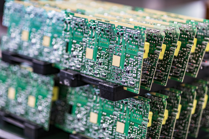
As the world of robotics advances, PCB manufacturing techniques have become faster and more efficient. With surface mount technology, flexible PCBs, multi-layer PCBs, advanced materials, and automation in PCB manufacturing, assembly techniques have drastically improved.
As a result, the robotics industry has seen the enhancement of component placement accuracy, thermal management solutions, and signal integrity. With these advancements, new possibilities become available, such as the design and production of circuits and products for a variety of industries and applications.
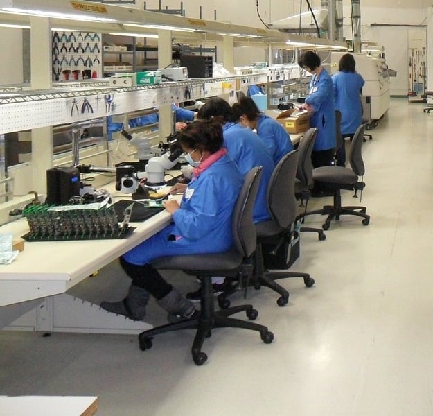
The use of robotics has greatly increased the speed of PCB production while also maintaining quality standards. This combined with advanced material usage has resulted in complex designs that complete their tasks efficiently. Additionally, many electronic companies are beginning to use automated systems with direct programming capabilities as a way to quickly test new ideas or concepts which can then be implemented on a larger scale with minimal cost.
We have previously gone in depth regarding Surface Mount Technology. For our purposes here, we will say that SMT involves placing components directly onto the board surface, rather than connecting them via holes in the board.
The benefits of SMT include:
 It’s fair to say that robotics have improved the capabilities of SMT since its introduction. Robots have improved productivity, accuracy, and reduced cost. Robots also have grippers that allow them to pick up smaller components, thereby allowing for more powerful PCBs to be constructed that take up less room in the intended product.
High-density interconnects (HDIs) offer greater miniaturization of PCBs. This specialized technology allows for more component placement in a smaller, confined space. In addition, HDIs also help reduce the amount of wiring needed for a board, making it lighter and more efficient. HDIs allow for higher levels of connection density than traditional methods, meaning more power is passed through each line while still taking up less space. With this greater efficiency comes enhanced performance, speed, and increased reliability.
HDIs can also increase the performance of the PCB by allowing for faster signal propagation and reduced crosstalk interference between pathways. By increasing efficiency and decreasing physical size, HDIs allow for the design of powerful and compact boards — perfect for applications such as laptops or mobile devices where space is at a premium.

Advanced materials like flexible substrates and high-frequency materials are used increasingly in PCB manufacturing for robotics. Flexible substrates allow robots to have complex movements while high-frequency materials aid in the miniaturization of PCBs. Experimental use of advanced materials also offers new opportunities for robotic design, such as improved thermal stability and better resistance to harsh environments.
These features can be especially beneficial when robots deploy in hazardous or extreme conditions, where they perform reliably for extended periods. For example, ultra-thin flexible substrates enable engineers to design higher-performance robots with more maneuverability. In addition, these advanced materials offer several advantages in terms of cost-effectiveness and fast production speeds compared to traditional PCB manufacturing methods.
Additive Manufacturing provides a powerful set of tools for designing and manufacturing custom, complex PCBs. By layering materials on top of each other, engineers can create intricate designs with highly accurate dimensions - in shorter amounts of time and with less waste.
This is especially beneficial for miniaturized PCBs, where the advanced materials enable them to be thinner than ever before while still providing the same level of performance. Additive techniques can also reduce production costs and increase production speeds compared to traditional methods like lithography.
IoT integration is becoming increasingly important for PCBs that are designed for smart robotics. By incorporating IoT in the design, PCBs can facilitate communication between the robot and a wide range of devices and sensors to provide it with information about its environment. For instance, using IoT-enabled PCBs, robots can be equipped with sensors that enable them to recognize objects in their vicinity without relying on a human operator.
This could contribute to greater safety and efficiency when working in dangerous environments. Furthermore, by integrating IoT into the PCB design of robots, they can become more adaptive and intelligent due to the ability to connect with different types of sensors that allow them to interpret their surrounding environment more accurately.
In the automotive industry, some robots have been outfitted with IoT-enabled PCBs to help assemble cars. For instance, car manufacturers like BMW, Toyota, and General Motors use these robots to accurately place parts in the right spot with minimal human intervention.
Meanwhile, in the healthcare sector, medical robots have been designed with IoT-enabled PCBs that can detect vital signs and send alerts when abnormalities are detected. One example is the Da Vinci robot, which is used for minimally invasive surgeries such as prostatectomy and hysterectomy. By leveraging IoT-enabled PCBs, this robot has helped reduce the time for surgery while improving the accuracy of diagnoses and treatment outcomes.
Overall, the use of IoT-enabled PCBs in robots has dramatically changed the way industries operate. In the automotive sector, these robots have helped reduce production time with greater precision and accuracy. Meanwhile, in healthcare they have improved the quality of diagnosis and treatment outcomes with minimally invasive surgeries. Ultimately, IoT-enabled PCBs are set to revolutionize many other areas of industry as their capabilities continue to expand and their applications become increasingly ubiquitous.
Matric staff can offer guidance on the best materials, processes, and timelines for PCB manufacturing. Consider this resource for more information:
1 min read
Printed circuit boards (PCBs) have been instrumental in the rapid advancement of technology since their introduction in the 1940s. PCBs...
1 min read
Consolidating services is a great way to reduce costs, lead times, & confusion. Unfortunately, most electronics contract manufacturers (ECMs) don’t...
1 min read
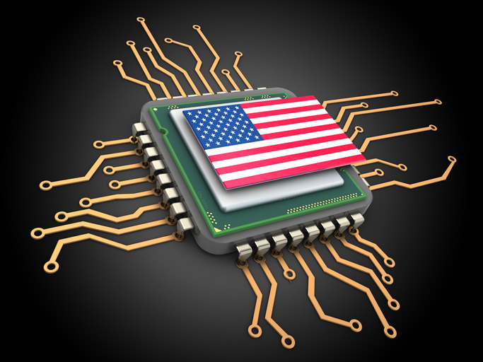
The global microelectronics industry is vital to the modern economy, with over $400 billion in semiconductor sales in 2020. As the demand for...