1 min read
Latest Advancements in Robotics & Current PCB Manufacturing Techniques
As the world of robotics advances, PCB manufacturing techniques have become faster and more efficient. With surface mount technology, flexible PCBs,...

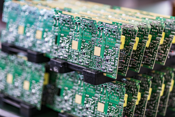
Printed circuit boards (PCBs) have been instrumental in the rapid advancement of technology since their introduction in the 1940s. PCBs revolutionized electronics by providing a compact, standardized platform for mounting and interconnecting electronic components. This innovation allowed for the miniaturization of electronic devices, paving the way for smaller, more portable gadgets that we now take for granted.
The evolution of PCBs enabled the development of more complex and powerful electronic systems. At the same time, the ability to design and manufacture intricate PCBs has been crucial in supporting the exponential growth in computing power and the emergence of new technologies. We will look at the introduction of PCBs and the devices that came into existence as a result. From there, we can dive into how technology improved and allowed more intricate PCB layout capabilities. These, in turn, set in motion today’s technological revolution, with improvements planned to continue well into the future.
The first functional PCB was created in 1941 by Viennese engineer Paul Eisler, who utilized a copper foil layer attached to an insulating board. He later used his PCB design in a radio that became crucial to military operations as it was paired with rockets to provide more efficient tracking. By 1948, the United States made the use of PCBs in airborne instruments mandatory.
This measure in turn led to the development of the auto-assembly process by US Army Signal Corps members in 1949, which was patented in 1956 and has become the fabrication process used to manufacture PCBs today. The process, called through-hole assembly, attached components to the board through pre-drilled holes.
Development continued to improve in the 1960s, with new materials included, like resins, which allowed quicker and more efficient printing methods. This also allowed for higher print volume at one time - although PCBs remained single-sided products. While still single-sided, they became multi-layered, with three or more layers of conductive material put to use, saving space and increasing flexibility. Soldering improved with the introduction of hot-air methods, which also helped improve the repair process.
Fast forward slightly to the 1980s and PCBs gained popularity in electronics. At this point, demand for smaller circuits grew, which has only increased over time. Surface mount technology (SMT) was brought into play to accommodate the demand for smaller circuits. This method, discovered by IBM, was already introduced in 1960 but was only found useful at this point in the PCB timeline. SMT is a competitor of through-hole assembly, speeding up production but also increasing the risk of issues with smaller PCBs that take up less space.
The military and aerospace industries were the top users of PCBs in the 1960s to 1980s. Communication was the top priority for the US during the Cold War with Russia post World War II. Meanwhile, space was the next focus, with the hope of making significant strides. Two of the main considerations for spacecraft were energy and weight restrictions. With the complex operations of PCBs and their comparatively small size and weight, they were the perfect addition to the space program’s toolkit for space exploration.
Early computers for consumers were also in production. However, these computers were bulky and offered limited operation compared to the significant price tag. Computer production was still in the early stages, and limitations due to the components available dictated size and capability.
Vacuum tubes were in use in the 1940s and were part of the first generation of computers. These took up significant space and required much larger boards to accommodate them. The tubes acted as switches, controlling the electricity flow and needed extensive cooling systems to keep them working correctly. Luckily transistors replaced vacuum tubes in the late 1940s and were key to the smaller size and increased efficiency of the second generation of computers.
 At that time, however, resistors, capacitors, and transistors were all still much larger than their counterparts that are in use today. These components were able to be mass-produced, even at the larger size, making them more affordable.
Some other issues for early PCBs were:
These limitations significantly influenced electronic devices' complexity, size, and capabilities during this period. The subsequent decades saw rapid advancements in materials, manufacturing processes, and design tools that helped overcome many of these constraints, leading to today's highly sophisticated PCBs.
The world of electronics manufacturing has come a long way since the early days of PCBs in the 1940s. SMT was refined in the 1980s to revolutionize the industry. Let's explore how SMT has transformed electronics production, offering significant advantages over its predecessors.
 quality and reliability that was difficult to achieve with manual assembly.
The shift from traditional PCB production methods to Surface Mount Technology represents a significant leap forward in electronic products. As we continue to demand smaller, faster, and more complex electronic devices, SMT will undoubtedly play a crucial role in meeting these challenges, just as it has revolutionized the industry since its widespread adoption in the 1980s.
3D-printed electronics are becoming increasingly popular, and the trend is expected to continue. During the 3D printing process, software controls material placement. The material types that can be used during 3D printing are widely varied and include:
These materials are applied layer by layer to create a finished component that can be designed to fulfill specific requirements, such as size restrictions.
This can all be accomplished in a much shorter time frame, therefore increasing 3D printing’s appeal as it improves customer satisfaction due to:
Over a span of less than a century, PCBs have made significant strides from introduction to today’s agility and customization. The reductions in size and increase in complexity have opened up opportunities for countless industries, with only more potential in the future.
Engineers have regularly identified and resolved pain points in the PCB production process, leading to the technological breakthroughs we see on a regular basis. Therefore, it pays to keep track of new innovations in agile PCB development, something Matric Group regularly does by investing in new equipment.
Seeking a better understanding of PCB manufacturing and how Matric can help you take advantage of today’s technology? Consider this resource:

1 min read
As the world of robotics advances, PCB manufacturing techniques have become faster and more efficient. With surface mount technology, flexible PCBs,...

1 min read
PCBs are crucial to modern financial systems and play a critical role in the infrastructure that supports the global financial ecosystem. These...

1 min read
Mining operations today rely heavily on precise, real-time data to ensure safety and efficiency. Printed circuit board (PCB) sensors have become...