


 Matric Group
‘Intrinsically Safe’ Design Guidelines for Electrical Devices
 Matric Group : Jul 16, 2020
Electrical devices that are safe to use in hazardous environments must abide by intrinsically safe design guidelines. Learn more about safe PCBs here!
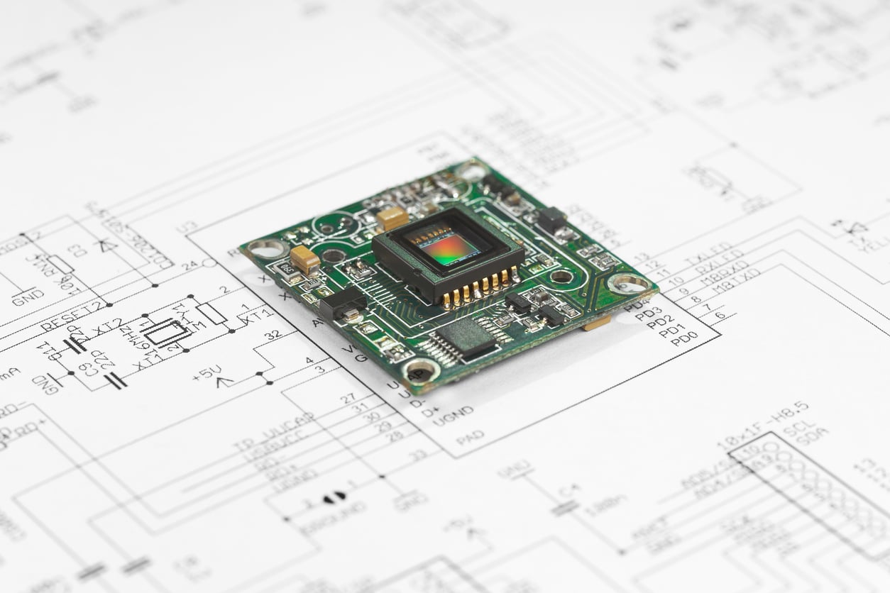
“Which standards apply to my project?” It’s one of the most common, and critical, questions engineers face when starting a new PCB layout and design. With multiple IPC (Association Connecting Electronics Industries (formerly Institute for Printed Circuits)) standards, evolving regulations, and industry-specific requirements, the answer isn’t always straightforward.
Getting it wrong can be costly. Misalignment with PCB design standards often leads to redesign cycles, manufacturing defects, failed audits, and delayed product launches. In high-stakes industries like medical, aerospace, and industrial systems, these risks can escalate quickly.
As technologies advance and compliance requirements grow more complex, aligning with the right printed circuit board standards from the start is no longer optional. Engineers who incorporate IPC standards for PCB designing and proven best practices early in the process are far more likely to deliver reliable, manufacturable designs on time and within budget.
PCB design standards are a set of established guidelines that define how printed circuit boards should be designed, laid out, manufactured, and inspected. These standards ensure that designs meet expectations for performance, reliability, and quality across the entire product lifecycle.
At their core, PCB design standards exist to:
These standards typically fall into four main categories:
By following these categories of pcb design standards guidelines, engineers can reduce risk and streamline the path from concept to production.
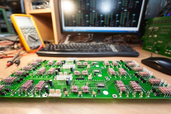
IPC is the leading global organization that develops standards for the electronics manufacturing industry. Its guidelines are widely recognized and adopted across industries, making IPC standards the foundation for modern PCB layout and design.
These standards provide a shared language between engineers, designers, and manufacturers, ensuring that expectations are clearly defined and consistently met.
Some standards directly guide PCB design, while others establish the fabrication, assembly, and acceptance criteria engineers should account for during design.
Key standards include:
Aligning with IPC standards for PCB designing provides several key advantages:
For engineers, IPC compliance is one of the most effective ways to ensure designs perform as intended from prototype through production.
Beyond formal standards, engineers rely on a set of widely accepted PCB design rules to guide development. These rules directly impact performance, reliability, and manufacturability.
Key considerations include:
Following these standard PCB design rules helps engineers avoid common pitfalls and ensures alignment with broader pcb design standards.
Effective PCB layout is essential to achieving both performance and manufacturability. Strong PBC layout guidelines focus on:
A well-planned layout not only improves performance but also simplifies manufacturing and inspection.
In many applications, PCBs must operate in challenging environments. Designing for reliability requires attention to:
Material selection, board thickness, and protective coatings all play a role in ensuring the PCB meets its intended lifespan.
Even experienced designers can encounter issues if best practices are overlooked. Common mistakes include:
Avoiding these issues is critical to maintaining compliance with pcb layout and design standards.
There is no single universal pcb size standard. Instead, board size is determined by a combination of design and manufacturing factors.
Key influences include:
Engineers must balance these factors carefully. While smaller boards can reduce material costs and fit compact designs, they may introduce challenges related to thermal performance, signal integrity, and manufacturability.
Understanding these trade-offs is essential when applying printed circuit board standards to real-world designs.

Selecting the right pcb design standards depends on the specific requirements of your project.
Important factors to consider include:
Early alignment between design and manufacturing teams is critical. By identifying the correct standards upfront, engineers can avoid costly changes and ensure the design meets all performance and compliance expectations.
Failing to follow pcb design standards can have significant consequences throughout the product lifecycle.
Common risks include:
In high-reliability applications, these risks are amplified, making adherence to pcb design standards guidelines essential from the beginning.
PCB design standards are the foundation of reliable, manufacturable, and high-performing electronic products. By aligning with IPC standards for PCB designing and following proven pcb layout guidelines, engineers can reduce risk, improve efficiency, and deliver designs that meet both technical and regulatory requirements.
For complex or high-stakes projects, partnering with an experienced manufacturer like Matric Group provides an added layer of confidence. With deep expertise in printed circuit board standards and a commitment to quality, Matric Group helps engineers get it right the first time, so designs move smoothly from concept to production.

 Matric Group : Jul 16, 2020
Electrical devices that are safe to use in hazardous environments must abide by intrinsically safe design guidelines. Learn more about safe PCBs here!
 Matric Group : Oct 30, 2020
When it's high in the sky, your aerospace PCB assembly better work as you intended. Never launch a project without this electronics aerospace design...
 Matric Group : Mar 26, 2020
PCB board firmness is an important design consideration. Don’t start production without an analysis of rigid PCB vs flexible PCB pros/cons for your...