


 Matric Group
1 min read
HDI PCBs For Medical Device Electronics Design
PCBs have been getting smaller for the past few decades, and few industries have taken more advantage of that than the medical industry. While...

There comes a day in nearly every engineer’s and buyer’s lives when they need a printed circuit board (PCB) for their company’s next electronic product. Whether you have a working knowledge of PCB layout design or are a newbie, it helps to grasp the start-to-finish journey a design makes.
Here’s some helpful insight into what to expect with a PCB project -- from how you’ll design it, to the steps involved, to who you should be paying to do it.
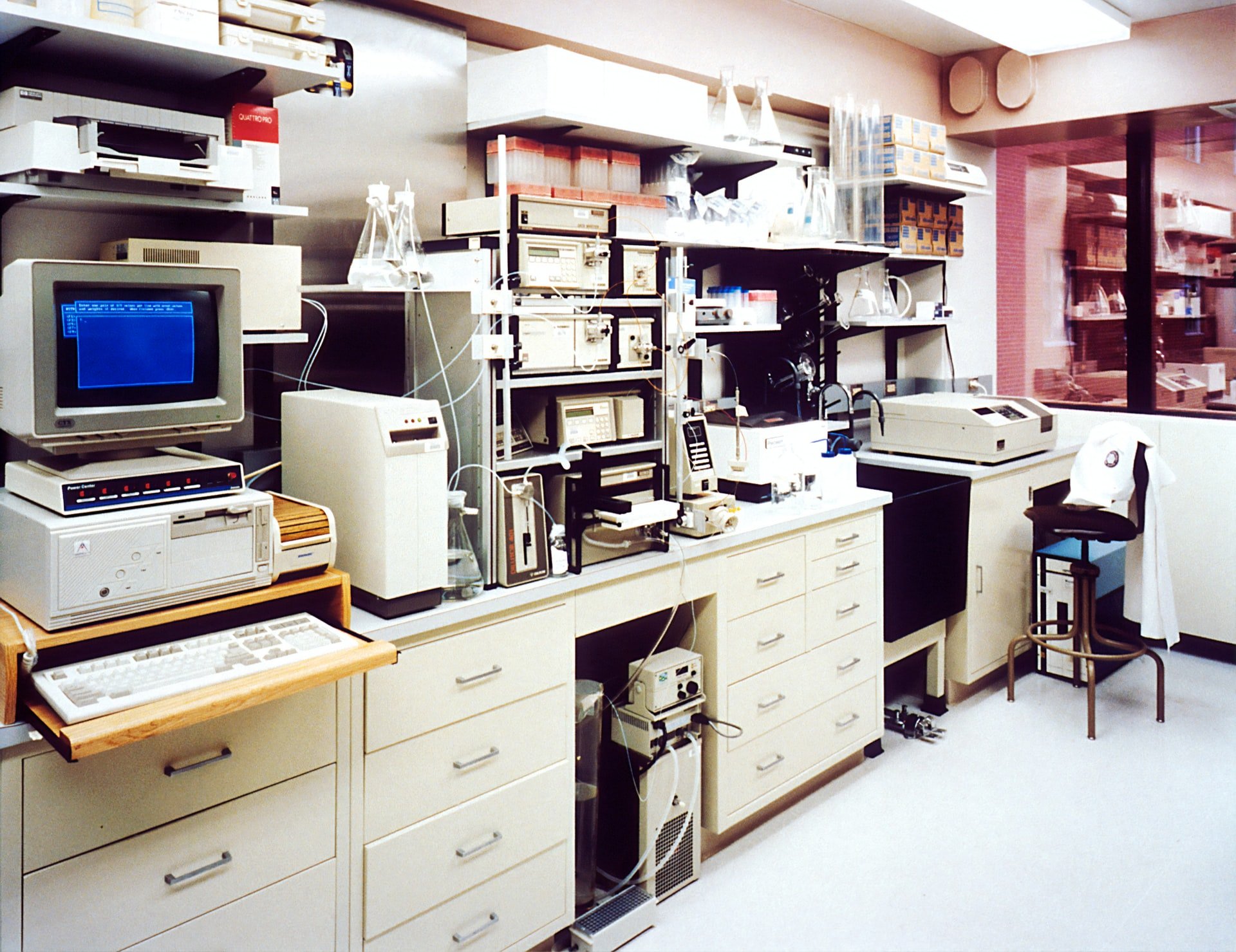
Printed circuit boards hold integrated circuits (ICs), transistors, and resistors -- and carry out the connections between them. A PCB lets you route power and signals between physical devices.
Connecting those boards and tiny components is solder. This miracle metal not only makes the electrical connections, it also serves as a strong mechanical adhesive. If your PCB is a slice of lasagna, the soldering is the sauce and ricotta cheese, while the boards are your layers of noodles.
Needless to say, PCBs are kind of important (though less tasty than lasagna). Whoever executes your design is going to need a robust program, especially if your layout is highly layered or otherwise complex.
Here are two programs we see come up often:
This is a conversation that pops up frequently between electronics companies and their board suppliers. Typically, the buyer is all about the free software, usually Eagle, while electronic design manufacturers (like us) prefer Altium.
(Note: Having been bought by software giant Autodesk, Eagle now offers a paid subscription version of its PCB layout software)
The problem with free software is that it can only do so much.
For example, Altium has no limit on the number of layers you can design in. Eagle has a four-layer limit.
Another example: Altium has no limit on a design’s size. Eagle has a size limit of 160 sq cm (though size is unlimited in the premium version).
So, unless you want a bare-bones design, you’re better off paying for a high-end suite of tools.
Here’s how the design process should play out with a well-versed vendor:
And there you have it: Your PCB baby is born.
Are you outsourcing your PCB layout design? For OEMs already outsourcing their manufacturing, seeking third-party help in the design phase could prevent a headache. Why?
Other than the obvious price factor, your choice of vendor will probably boil down to two words: capacity and capability.
For starters, what level of volume is your project? Some contract manufacturers will also accept low-to-mid-volume capacity jobs. Other, major companies want only the highest-capacity work.
Complexity also commonly separates one vendor from another. Some can handle complex, multilayer boards. Others stick to simple designs.
Even more important: Most electronic contract manufacturers can’t do both in-house PCB design and assembly.
The few vendors that are one-stop shops can take your project from inception to finished product. What does this mean for the customer?
Well, if a design issue is noticed during the assembly process, a company with only assembly capabilities will struggle to resolve the problem. This is why it also helps to go to a company that offers extensive testing and prototyping services. It’s always better to make a mistake during these stages than discover one after your boards are already shipped.
Other benefits of using a single source of electronic manufacturing:
Hopefully you’re now wiser to the standards you should have when using PCB layout design. Choosing the right software, understanding the manufacturing process, and picking a vendor with appropriate capabilities will make your job easier.
For more tips on succeeding with electronic manufacturing, check out this article on the need for certain products to be intrinsically safe.
1 min read
PCBs have been getting smaller for the past few decades, and few industries have taken more advantage of that than the medical industry. While...

1 min read
The electronics sector is one of the most dynamic industries, with virtually unlimited applications. This is why its growth is expected to remain...

1 min read
You’ve heard about the many great feats and discoveries in the aerospace industry. You’ve also heard about the tragedies that have happened when a...