


 Matric Group
1 min read
HDI PCB Design Guidelines for Layout & Manufacturability
Want to get smaller, lighter, or more powerful? (Who doesn’t?) In electronics, customers are demanding all three – at the same time. It might seem...

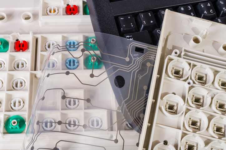
In every facet of modern life, we're surrounded by electronic devices, all of which are powered by printed circuit boards (PCBs). With so many devices constantly emitting electronic signals in close quarters, the question of electromagnetic interference becomes a crucial one.
We're going to analyze how interference affects printed circuit boards. Then we’ll share our favorite electromagnetic interference (EMI) reduction techniques in PCB design that help regulate, limit, and eliminate sources of interference.
EMC stands for electromagnetic compatibility. The term is often used interchangeably with EMI, which stands for electromagnetic immunity. While the two topics are not exactly the same, discussion about one goes hand in hand with the other.
Although they share the same acronym, electromagnetic immunity should not be confused with electromagnetic interference. Interference is the amount and intensity of radio emissions that a device radiates. Immunity is the ability of neighboring devices or components to withstand that radiation without having their functionality impacted. Types of interference include:
EMI is therefore a subset of EMC. EMC encompasses both interference (radio emissions) and the level of immunity of neighboring electronic or internal components. EMC standards for PCB design refer to the circuit board's ability to withstand radiation from other noise-producing elements within the device itself and its penchant for producing disruptive emissions of its own.
Because personal electronic devices are ever-present in our daily lives, device manufacturers must follow certain design considerations. Otherwise, consumers would face an intolerable amount of radio interference anytime multiple devices come into contact with one another. Fostering a sufficient level of EMC begins with accounting for EMI protection in your PCB design.
Below are some circuit board manufacturing best practices to ensure that your PCB meets EMC standards for PCB design and functions to the best of its capability.
Almost every circuit board employs some form of ground plane. It's a common element of any electronics design guide.
In multilayer PCB design, a complete layer covering the board's entire surface is dedicated to grounding and serves as the primary configuration for reducing electromagnetic interference. A ground plane's sole purpose is to reduce or eliminate interference and noise between all of the board's individual circuits, and is highly effective for improving the PCB's compatibility level.
When it comes to EMC design, there's no better way to reduce electromagnetic interference than by optimizing your PCB layout. Circuits that cross or are clustered in close proximity are a prime source for radio emissions. Certain types of circuits are more susceptible than others, including:
One key way to mitigate noise through PCB layout is to maintain separations between traces. When possible, arrange circuits in differential pairs in a technique known as guarding. This can reduce emissions and cross-talk in high-speed circuit lines.
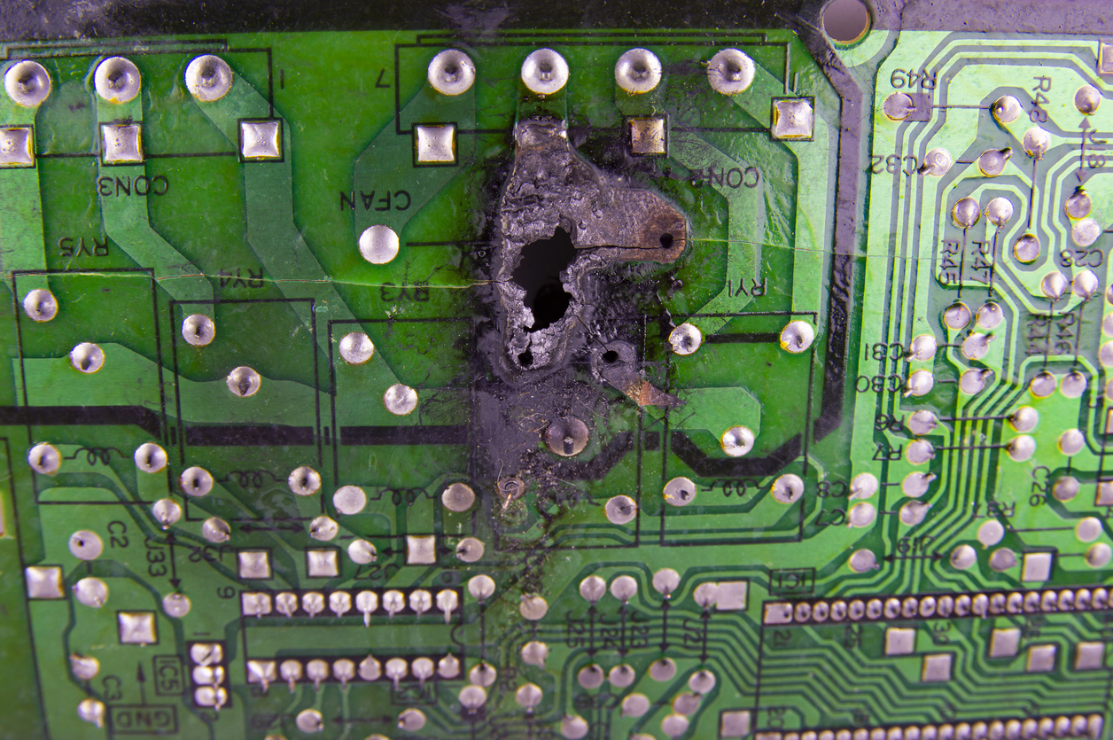
Another major source of interference is a sudden spike, change, or disruption to the power supply. To prevent harmful surges from occurring, your PCB design should include the use of components like transorbs, also known as transient voltage suppressor diodes, and metal oxide varistors (MOVs) that can mitigate sudden shifts from the power supply.
Electrostatic discharge is always a concern when working with devices and components that bear an electrical charge. Should the components in question come into contact with an oppositely charged item, they can produce a destructive shock.
When designing a PCB, take the time to employ some form of ESD protection. The intervention that you choose will differ depending on the application of your PCB. It may be in your best interest to partner with a third party to help you design a bespoke ESD protection component.
While you should always begin with logical board design (addressing the basics, like grounding all applicable cables), you can also employ PCB EMI shielding design as a final line of defense against RF emissions.
Note that metal makes a far more effective shielding material than plastic. Plastic transmits many RF frequencies, whereas a metal sheathing over your PCB will block the RF emissions from spreading.
It's essential to understand how international EMI standards for PCB affect the design of your circuit board.
If you're working with a US-based PCB manufacturer, the FCC oversees emissions standards for your manufacturing operations. However, if your circuit boards don't employ a clock, some form of power switching circuits, or a low-frequency digital signal then FCC standards don't necessarily apply.
CE, on the other hand, is a European standard that denotes that an electronic device meets certain standards of health and safety. Regardless of power source, all electronics require CE testing. The good news is that both the FCC and the CE are comparable when it comes to emissions testing, so when you design for one, you design for both.
Both the FCC and CE testing standards apply to a range of electromagnetic interference-related issues, such as:
In many cases, the respective standards that address each category revolve around the finished product rather than the PCB itself, but due to questions of EMC and mitigation, it's good to have cursory knowledge nonetheless.
Testing for the level of electromagnetic compatibility is generally a three-part process. The standard tests come first, followed by a more specialized level of emissions testing. Three core tests that help you gauge the EMC of your PCB include:
While these three tests are by no means inclusive, they represent a good cross-section of essential testing methods to ensure that your PCB has a high level of electromagnetic compatibility.
Designing a PCB is equal parts technical acumen and artistry. There are dozens of factors to consider, from official EMC standards for PCB design to general best practices for EMI reduction techniques for PCBs.
Make sure you follow good, sound PCB design guidelines for reduced EMI. That way your product will "play nicely" with the other electronic devices it will inevitably encounter.
To learn more about testing your PCB for durability and safety, check out our free e-book:

1 min read
Want to get smaller, lighter, or more powerful? (Who doesn’t?) In electronics, customers are demanding all three – at the same time. It might seem...
1 min read
The products that your organization is preparing to develop call for printed circuit boards (PCBs) -- simple enough, right? Not exactly. Components...
1 min read
Printed circuit boards (PCBs) are the backbone of nearly every electronic device. From industrial controls and medical equipment to defense systems...