


 Matric Group
1 min read
Why PCB Failures Happen: 6 Common Causes OEMs Can Prevent
Printed circuit boards (PCBs) are the backbone of nearly every electronic device. From industrial controls and medical equipment to defense systems...

Telecommunications PCBs (printed circuit boards) are a different breed. As you'd expect, you’ll need to reconsider everything you thought you knew about PCB layout and design to cater to this fast-moving industry.
It's not just the materials that are different -- other aspects, like testing, are also going to be different. You'll also need to deal with other factors potentially out of your hands, like tight deadlines and tighter budgets.
Buyers expect telecommunications electronics designs to help them connect with the world more quickly, clearly, and efficiently. Here's a quick run-down of the PCB design considerations you need to factor in for your product to make it to market.
Telecom PCB design considerations begin well before your manufacturer places the first component on the board. You have to consider these aspects right out of the gates:
Once you have the answers to the above questions, you can start the design process.
To help your electronics contractor get you a telecommunications product on time and on budget, consider the following:
PCBs have no shortage of applications in the telecoms industry:

Understanding how the final product works, its problems, the target users, and the desired features will go a long way in influencing the PCB design.
How the device is powered will also affect the PCB design. Some power options might require an interface, as well as any possible connectors.
Don't forget the fundamental aspect of product size, which will also determine the size of the PCB.
A careful analysis of the final product will prevent hiccups in the next stage of production.
Depending on the PCB’s function, you can add select hardware components to complete some functions. Alternatively, you can add code to the software of the device.
This is one of the most critical PCB design considerations, and one that will have far-reaching repercussions. You’ll need to determine if software can achieve the desired functionality. If not, what kind of hardware will you need? If both options are feasible, consider the advantages of each.
For the hardware:
For software:
The microcontroller is an essential part of the PCB design. It's the "brain" of the product, receiving and transmitting input to and from various components. If the PCB is for telephone switching systems, the microcontroller is even more important because it's the desired choice for communicating with individual switches and other essential hardware components.
Some of the factors to consider when choosing a microcontroller include:
Don't forget the technical considerations as well, which will cover the architecture and the hardware and software programming tools required to get the microcontroller running.
After going through the above steps, your PCB should start coming alive. You have a better idea of the components you need, so you can start working on the schematic.
The schematic should include details like
Ensure you have sufficient space on the bare board to fit all necessary components.
Refer to a PCB layout design guide to make sure every spec is applied wisely and avoid issues in the stages that follow.
Also, remember to add enough soldering mask between every pin on the board, especially for components in microscopic packages. Keep in mind that inadequate soldering mask is one of the leading printed circuit board layout defects.
Like every other step of the telecom PCB design process, there are durability and performance concerns with component placement and routing:
Once you outline the components and interconnecting positions, your manufacturer should start placing the individual components, followed by an analysis for any potential adjustments to routing and performance. For the best results, consider placing components in a particular order:
Best practices for component placement include:
Finally, it’s time to run quality checks on the completed PCB! Have the PCB thoroughly reviewed and collect feedback from all the other designers involved in the project. Keep a detailed list of all changes.
Use readily available tools like a Design Rule Checker to avoid design errors and an Electrical Rules Checker to ensure it addresses all specifications and constraints.|
Telecommunications electronics design is a high-stakes and quick-paced world. With projects often hitting seven figures or more, PCB testing takes on even more importance.
To learn more about PCB testing and prototyping and how they help influence your design considerations, download the free e-book below:
1 min read
Printed circuit boards (PCBs) are the backbone of nearly every electronic device. From industrial controls and medical equipment to defense systems...
1 min read
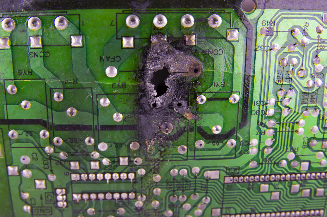
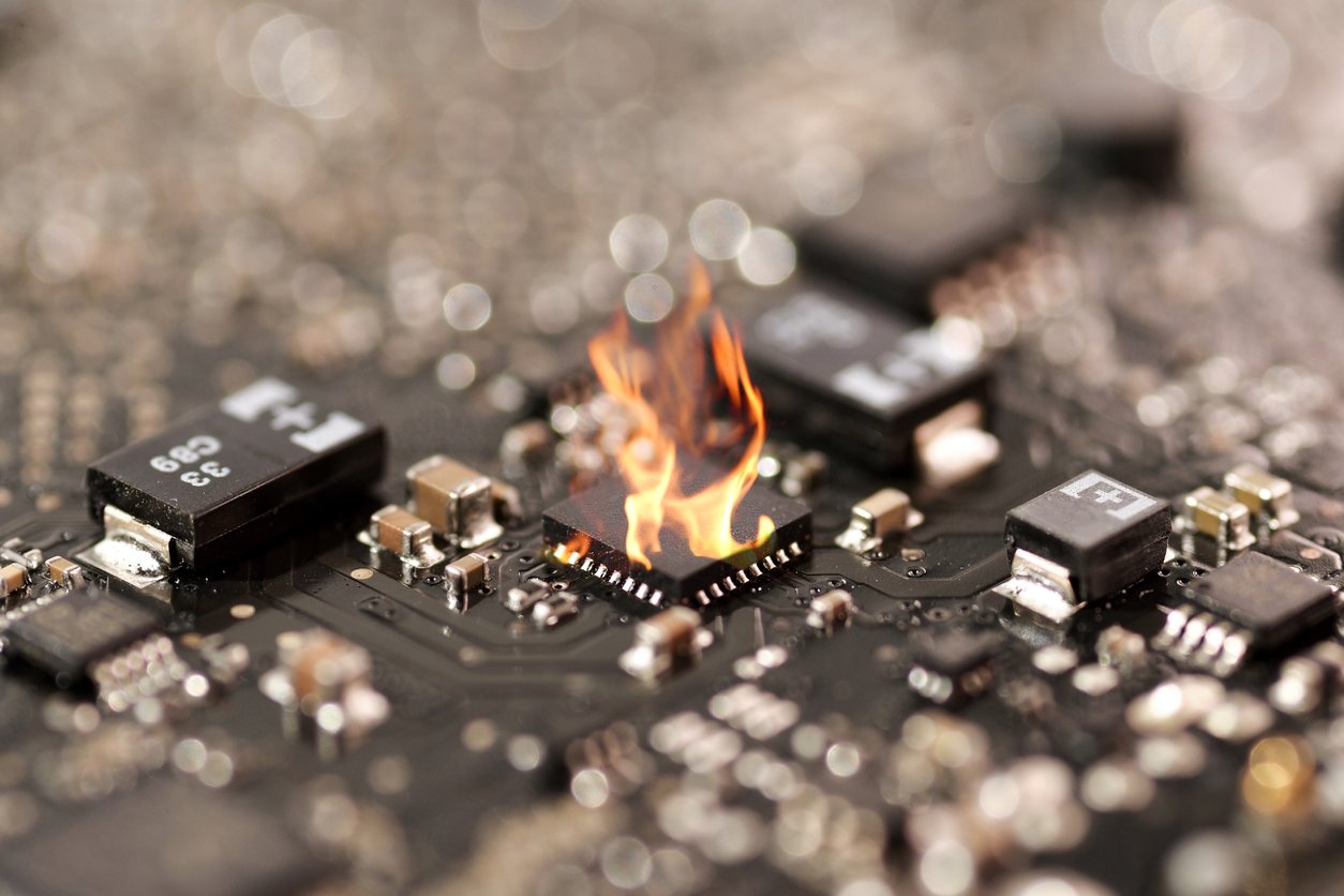
While there are many common printed circuit board defects, one of the most notorious is burnt components. It's also, unfortunately, one of the most...
1 min read
Prototyping isn’t reserved for high-tech vehicles or revolutionary consumer gadgets. It’s also a great practice for manufacturing printed circuit...