


 Matric Group
1 min read
How to Tell Tombstone PCB Defects ‘Rest in Peace’
Working with small circuit board areas can increase the risk of various PCB defects, tombstoning in particular. While the grim nature of...
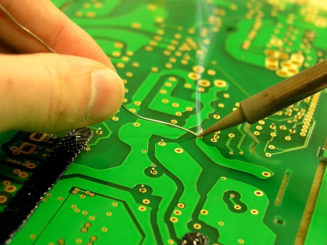
Printed circuit boards are vital components of many modern-day electrical gadgets. Printed circuit board layout is made up of numerous layers of copper traces and circuits that help make connections between various parts, as well as plastic and other types of materials that are used to cover and shield the connections from the surroundings.
How you design and manufacture printed circuit boards (PCBs) largely determines how well these boards will work in the final product. Unfortunately, layout is becoming increasingly difficult and complicated, as new board circuit designs are being shrunk to fit in electrical devices that become becoming smaller and smaller each year.
If you choose to design your PCB in-house, avoid the following possible layout issues because they can be costly and may lead to a defective product. Also, ensure that you have a design-for-test strategy, get a design review from an independent engineer before producing prototypes, and involve your manufacturing vendor early in the process to avoid design-manufacturing incompatibility.

Plating voids and gaps are holes in the plating of the circuit build as a result of an imperfect deposition process. Plating voids are a problem because they prevent electrical current from flowing through a through hole to the other side of the circuit board. And without a complete flow of current, a device cannot function as required.
Plating voids occur because the copper used does not coat well during the electroplating and deposition process. This may happen as a result of material contamination, inadequate catalyzation of copper during deposition, inadequate cleaning of through holes, air bubbles present in the material, or rough drilling. You can avoid these defects by correctly drilling through holes according to the board’s manufacturer instructions and then cleaning the material well after that.
Slivers are thin wedges of soldering mask or copper material generated during the etching process and can have a diverse impact on a PCB’s functionality. It can occur in two ways. One, it can happen when long, thin copper or solder mask detaches before completely dissolving in the chemical bath. The slivers can get attached to another board and create an unwanted connection which can lead to a short and hence defective circuit board.
Two, slivers can be produced when a section of the PCB is cut too thick or too thinly. The slivers can detach entirely or just peel back, potentially resulting in corrosion of copper material as time passes. You can evade creating slivers by designing sections with smallest widths.
When your PCB’s solder mask (the coating over the surface meant to protect the copper) is partially or fully missing between pads, more copper than necessary is uncovered. This can lead to solder bridges developing between pins when the board is in assembly.
When you design a PCB for a fine pitch device, for example, some designers will say, “We don’t really need a mask in here!” But we find ditching mask makes it easier for bridging to occur during the manufacturing process. Sometimes you’ll also find that if there’s two pads that need joined and there’s a missing mask, it’ll look like there’s a bridge when there’s not.
Failure to use a mask can result in a short, as well as low corrosion protection, negatively affecting the functionality and durability of your board.
An acid trap commonly refers to an acute angle in the circuit board which can trap acid during the etching process. This acid stays here longer than it’s supposed to; eating away more than is required and compromising connections hence making a circuit defective.
You need to thoroughly check your design to make sure there are no acute angles present.
Too much electromagnetic interference can result in a product failing to function. Not surprisingly, this interference is often a result of flaws in the design process.
You can consider increasing grounding for the circuit board, avoiding 90-degree angles for most components, and utilizing shielding cables, and metallic packages for electromagnetic absorption. (To understand shielding cables, think of your TV cable -- there’s a conductor going down the center cable that’s got the TV signal on it. The outside ones protect it from interference, so when you turn your TV on, your kitchen blender doesn’t freak out.)
Placing copper too close to the edge of the circuit board can lead to numerous problems. The copper can cause a short if it comes into contact with another conductive material; it’s also left susceptible to corrosion.
We’ve seen designers even run a trace right off the edge of the board. The problem is that when your board house depanels the board and cuts it to dimension, it may completely cut the trace away, causing the copper layer to be exposed.
It’s not fun sinking a bunch of money into a board design and having the final product be completely useless because there’s no trace in it. While the board house may reimburse you for the board, it won’t do anything about the money you put into the board after the cutting.
You can avoid this problem by simply putting adequate space between both the copper and board edges.
Using inefficient layout techniques or incorrect components, failure to engage your manufacturer for DFM (design for manufacturability), failure to thoroughly test early prototypes, and lack of planning are other tricky situations you’ll see when creating printed circuit board.
To avoid all these issues, it’s sometimes better to outsource the job to PCB design experts and increase your odds of receiving a 100% functional circuit. This is especially true for jobs that are highly complex but not particularly high-volume.

1 min read
Working with small circuit board areas can increase the risk of various PCB defects, tombstoning in particular. While the grim nature of...

1 min read
You’ve heard about the many great feats and discoveries in the aerospace industry. You’ve also heard about the tragedies that have happened when a...
1 min read
Optimizing PCB layout design for manufacturability is one of the most crucial aspects of your product’s development process. Key decisions made...