


 Matric Group
1 min read
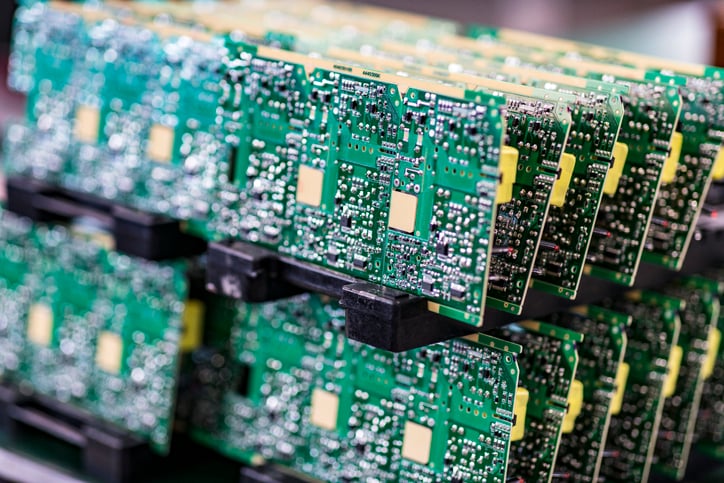
HDI PCB Design Guidelines for Layout & Manufacturability
Want to get smaller, lighter, or more powerful? (Who doesn’t?) In electronics, customers are demanding all three – at the same time. It might seem...

1 min read
Want to get smaller, lighter, or more powerful? (Who doesn’t?) In electronics, customers are demanding all three – at the same time. It might seem...
1 min read
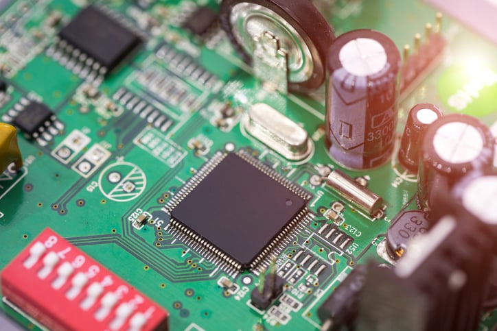
PCB (printed circuit board) costs are a concern for any electronics designers or manufacturers -- both the materials that go into PCBs and the...
1 min read
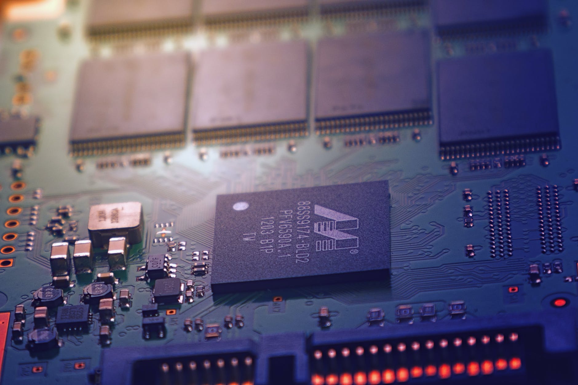
So, you’ve made the choice to design a custom PCB for your design. Instead of buying off the shelf electronics.. but what’s next?