


 Matric Group
1 min read
Financial PCBs 101: PCB Design For Trading Platforms
Driven largely by technological advancements and the increasing demand for efficient trading solutions, the financial technology landscape is...

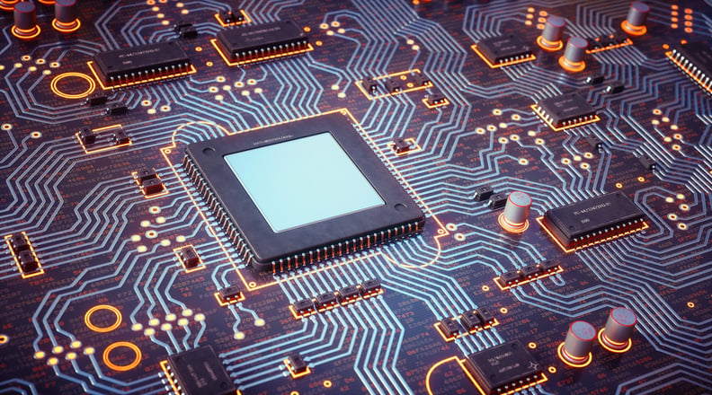
In the digital age, where transactions are often completed with a mere tap or click, the seamless operation of financial systems has become a cornerstone of our daily lives. An unsung hero lies at the heart of these sophisticated systems: the Printed Circuit Board (PCB). PCBs are the backbone of nearly all electronic devices, providing a platform for the compact and efficient assembly and connection of electronic components. In financial systems, these boards are critical in enabling the reliability and speed of payment processing systems.
Payment processing systems are the technological frameworks that facilitate financial transactions between buyers and sellers. They encompass a wide array of devices and software, including:
These systems ensure that transactions are conducted swiftly and securely, protecting sensitive financial information against potential threats.
The importance of PCBs in these systems cannot be overstated. They are designed to meet the rigorous demands of the financial industry, including high reliability and the ability to process transactions rapidly. Moreover, PCBs in payment processing systems must comply with strict security standards to safeguard against fraud and ensure data integrity.
As we delve deeper into the intricate world of payment processing systems, we'll explore how PCBs facilitate the complex operations that make instant, secure transactions possible. From the smallest chip card readers to the most sophisticated banking networks, PCBs ensure the financial world keeps spinning, underscoring their vital role in our interconnected, digital society. Join us as we uncover the technologies that make modern finance tick, highlighting the pivotal role of PCBs in the seamless execution of daily transactions.

PCBs have enabled the miniaturization of electronic devices while increasing their functionality. In payment processing systems, this means more sophisticated point-of-sale (POS) terminals, mobile payment devices, and ATMs that occupy less space and consume less power. Integrating various functionalities into single devices is made possible through the complex circuitry that can be packed onto a PCB, allowing for the support of multiple payment methods (such as magnetic stripe cards, chip cards, and contactless payments) within a single device.
The security of financial transactions is paramount, and PCBs contribute to this aspect by enabling the integration of advanced security features into payment processing hardware. This includes encryption modules, secure microcontrollers, and other security-focused components that protect against tampering and unauthorized access. The layout and design of PCBs can also be tailored to enhance the physical security of the devices, further safeguarding sensitive financial data.
Modern payment processing systems are part of a larger networked ecosystem, requiring reliable connectivity and communication capabilities. PCBs facilitate these requirements by including wired (Ethernet or USB) and wireless communication (Wi-Fi, Bluetooth, and NFC) components within payment processing devices. This connectivity enables secure, real-time transactions and the integration of payment systems with broader financial networks and cloud-based services for enhanced data analysis and management.
As payment technologies evolve and consumer preferences change, payment processing systems must adapt quickly. PCBs support this scalability and flexibility by allowing for easy updates and modifications to the hardware. New functionalities can be added through changes in the PCB design or by integrating new modules, ensuring that payment processing systems can keep pace with technological advancements without the need for complete hardware overhauls.
Furthermore, as payment systems become intertwined with increasingly complex digital ecosystems, PCBs will be crucial in facilitating seamless integration. This involves the physical integration of payment modules into a wide array of devices and platforms and ensuring that these systems can communicate effectively within the broader digital infrastructure.
For instance, integrating payment systems into the Internet of Things (IoT) devices, smart infrastructure, and even blockchain networks requires versatile, secure PCBs capable of efficiently processing large amounts of data.
Payment processing systems require high reliability and durability due to their critical role in financial transactions and constant use. PCBs are designed to meet these requirements through durable materials and manufacturing processes that ensure long-term reliability even under continuous operation. The design of PCBs also accounts for environmental factors, such as temperature and humidity, which could affect the performance of payment processing systems.
The evolution of payment processing systems, marked by increasing speed, reliability, security, and flexibility, owes much to the advancements in PCB technology. Modern PCBs are engineered to meet the exacting demands of the financial sector, incorporating features like multi-layer designs for enhanced circuit density, and specialized materials that can withstand the rigors of continuous operation. This has allowed payment processing devices to become:
The manufacturing process of PCBs for use in the financial industry is a meticulous procedure designed to ensure the highest levels of reliability, security, and performance. Given the critical nature of financial transactions, PCBs in this sector must meet stringent standards, from material selection to comprehensive testing. Here's an overview of this intricate process:
The process begins with the PCB design phase, where engineers use specialized software to lay out the circuit and select materials that meet the unique needs of financial applications. Material selection is crucial; high-quality, durable materials are required to withstand the continuous operation of payment processing systems and secure devices. Typically, materials with excellent thermal management, mechanical stability, and electrical performance are chosen, such as high-grade FR-4 for the substrate, and copper for conductive pathways.
Once the design is finalized, a prototype PCB is manufactured. This step allows engineers to identify any potential issues with the design or material choices before moving into full-scale production. Prototyping is critical for ensuring the PCB technology needs will perform as expected under the conditions it will face in real-world financial systems.
PCBs for the financial industry often require multiple layers to accommodate complex circuits needed for secure transactions. These layers are stacked and laminated under high pressure and temperature to create a single, integrated board. This step is pivotal for the structural integrity of the PCB.
Precise holes are drilled into the laminated PCB for mounting electronic components and establishing vias (electrical connections between layers). After drilling, the board undergoes a plating process to coat the holes and surfaces with a thin layer of copper, which enhances electrical connectivity and protects against corrosion.
A photoresist is applied to the board and then exposed to ultraviolet light through a mask that outlines the circuit pattern. The unexposed areas are removed and the exposed copper is etched away, leaving behind the desired circuit pattern.
Electronic components are placed onto the PCB and soldered to form secure, conductive connections. This step may be done manually for prototypes or using automated processes for high-volume production.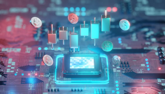
PCBs in the financial industry undergo rigorous testing to ensure they meet the required standards for reliability, security, and performance. This includes electrical testing to verify proper circuit functionality, thermal testing to create adequate heat management, and mechanical testing to assess durability. Additionally, security testing is paramount to confirm that the PCBs can resist tampering and hacking attempts, a critical consideration for devices handling financial transactions.
Finally, each PCB is inspected for quality assurance, ensuring it meets all industry standards and regulations specific to financial systems. This includes compliance with international PCB manufacturing standards and any additional requirements specific to financial devices, such as EMV (Europay, Mastercard, and Visa) standards for payment systems.
The manufacturing process of PCBs for the financial industry is designed to produce efficient and reliable boards that are secure against potential threats. PCBs are crafted to support the high-stakes world of financial transactions, ensuring the seamless operation of payment processing systems worldwide through:
Still looking for answers to your PCB assembly questions? Consider these additional resources from our blog library:
PCBs play a critical role in enabling financial advancements, serving as the essential foundation upon which these technologies are built and integrated into the ecosystem. The landscape of payment processing technology is rapidly evolving, with several key trends poised to redefine how financial transactions are conducted soon.
At the forefront of this transformation, each offering new levels of convenience, security, and efficiency are the following innovations:
Biometric authentication uses unique physiological characteristics, such as fingerprints, facial recognition, or iris scans, to verify individuals' identities. This method offers higher security than traditional PINs or passwords, reducing the risk of fraud.
PCBs are integral to the devices that capture and process biometric data, providing the necessary electronic circuits for sensors, data storage, and connectivity. Future PCBs will need to accommodate more sophisticated sensors and faster processors to improve the accuracy and speed of biometric authentication, necessitating advancements in PCB design and materials to handle the increased data throughput and power requirements.
PCBs in AI-driven payment systems must support high-performance computing components capable of processing vast amounts of data in real time. AI is set to revolutionize payment processing by:
This includes integrating specialized AI chips or GPUs (Graphics Processing Units) that can execute complex algorithms efficiently. As AI becomes more embedded in financial systems, PCBs will evolve to be more power-efficient, have higher thermal tolerance, and provide faster data connectivity to accommodate the intensive computational demands of AI technologies.
The IoT's expansion has enabled several devices to execute payments, from smartwatches and appliances to vehicles and smart city infrastructures. IoT payment solutions require PCBs to be highly compact, energy-efficient, and capable of secure wireless communication.
The future of IoT in payment processing will likely see an increase in the deployment of NFC and RFID (Radio-Frequency Identification) technologies, necessitating PCBs that can support these functionalities in a wide range of devices. Additionally, as IoT devices become more interconnected, the emphasis on security will necessitate PCBs to incorporate advanced encryption and secure element chips to safeguard transaction data.
As these technologies advance, the role of PCBs in payment processing systems becomes increasingly critical. PCBs must evolve to meet the new requirements of these technologies, such as supporting higher speeds, greater complexity, and enhanced security measures. This will involve innovations in PCB materials, manufacturing processes, and design techniques.
For instance, the use of high-speed signal materials, improved thermal management solutions, and miniaturization techniques will become more prevalent. Moreover, to ensure the security of financial transactions, PCBs must incorporate features that enable secure boot processes, encrypted communication, and resistance to physical tampering.
The future of payment processing technology, driven by advancements in biometric authentication, AI, and IoT, promises to make financial transactions more secure, efficient, and user-friendly. PCBs are fundamental to this future, providing the critical infrastructure to support these technologies.
PCBs serve as the foundational platform upon which the functionality and reliability of modern payment processing systems are built. These intricate assemblies house and connect the various electronic components that drive the machinery of financial services, from the microprocessors that handle encryption and decryption to the communication modules that enable devices to link with financial networks. The critical role of PCBs in financial systems, particularly with payment processing, is their ability to ensure that these transactions are swift, secure, and dependable.
PCBs stand at the forefront of enabling the technological advancements that drive the efficiency and security of modern payment processing systems. Their continued evolution will be instrumental in supporting the future of financial transactions, paving the way for adopting new payment technologies and integrating payment systems into the fabric of the digital age. As such, the development and innovation of PCB technology remain critical to the advancement and reliability of financial systems worldwide.
Want to learn more about PCB testing and standards? Consider this resource:
1 min read
Driven largely by technological advancements and the increasing demand for efficient trading solutions, the financial technology landscape is...

1 min read
PCBs are crucial to modern financial systems and play a critical role in the infrastructure that supports the global financial ecosystem. These...
1 min read
The electronics sector is one of the most dynamic industries, with virtually unlimited applications. This is why its growth is expected to remain...