


 Matric Group
1 min read
7 Types of PCB Soldering Defects to Watch Out For
Let’s face it, soldering can be a challenging task. Even with years of training and the most advanced machinery, PCB soldering defects are...
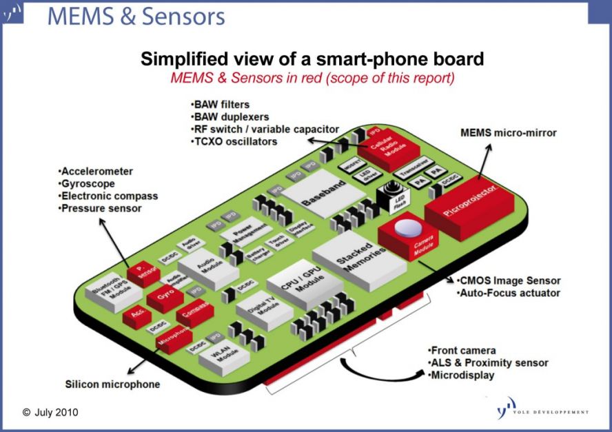
Microelectromechanical systems, or MEMS, are the microscopic building blocks of current electronics. Look no further than the smartphone in your pocket -- these tiny devices make up many of the sensors in our phones that collect data like motion and image stabilization.
These little pieces have opened up a world of possibilities for companies looking to innovate with their products and craft revolutionary new ones Here’s a quick-and-dirty MEMS design guide to help your PCB design for electromechanical assemblies compete with the best.
The driving force behind the development and use of MEMS is the continued miniaturization of electronics. As the demand for smaller electronics has grown, engineers needed to craft smaller components that still retained the ability to operate vital functions. MEMS not only achieve that goal, but also consume less power, leading to longer operating times.
Here’s an example of the impact of a MEMS component. A newly designed 6.9pf capacitor that began production in December 2018 can reduce the components necessary to generate the reference clock signal in a device, thus reducing the space required by 65 percent and giving design engineers more flexibility. This MEMS device is not only half the size of a traditional crystal resonator, but also consumes 13% less power.
(Image courtesy Yole Developpement)
Biomedical MEMS, also known as lab-on--chip (LOC), is a subset of MEMS. Technological developments such as whole genome sequencing projects and drug discovery created a demand for these devices.
For the most part, MEMS devices used in the medical field are similar to those used in others, such as:
Environmental
Aerospace
Consumer products
For example, a MEMS inertial sensor found in an airbag deployment mechanism is the same as one found in a pacemaker.
The Bio-MEMS field is notable for its ability to address health-related issues. For example, drug release technologies have the potential to completely control drug release, from automatic dosing to delivery to diagnostic feedback. Implantable drug delivery systems are now possible, like the microfluidic device doctors can now implant in eyelids to treat ocular diseases. Surgical microtools can lower risk during operations by providing real-time feedback to surgeons, identifying critical information like blood flows, tissue type, and oxygen levels.
Due to the stature of MEMS devices, they can be considerably fragile. Here are a few helpful tips to consider when designing your device:
MEMS motion sensors are sensitive to mechanical stress coming from the printed circuit board on which it will be placed. You can limit stress levels with the following:
Maximize symmetry and balance of pad connection. This helps with component self-alignment and results in better solder paste reduction after reflow.
Avoid non-RoHS-compliant compounds, especially leaded solder.
Shifting may occur after the sensor is mounted to the PCB. We recommended that you conduct an onboard calibration after the accelerometer is soldered.
Running traces underneath the MEMS package in not recommended. Routed active signals could harmonically couple with the MEMS sensor devices and impair their performance. To avoid this coupling, do not route signals directly above or below the MEMS package.
For optimal performance, use ground planes underneath the sensor to reduce PCB signal noise. If there is an adjacent PCB in the assembly, consider mounting one above the package as well.
MEMS sensors need their space. Some components like large insertions can cause stress to the motion sensor if placed within 2 mm of the device. Be sure to follow accepted design standards around MEMS devices to limit the amount of mechanical stress it suffers.
Surface mount technology should be used when placing a MEMS device. Typically you should employ a pick-and-place machine that connected to a reflow oven. We recommend you do not manually solder MEMS devices as this could have adverse effects on the package.
A full-service electronic contract manufacturer should have the ability to both design and produce MEMS PCB assemblies. Bonus points if your ECM has an in-house engineering team that can develop a design that optimizes its functionality and manufacturability.
For example, our four SMT lines can handle any size production order. If you’re interested in learning how a electronic manufacturing services partner should assist in your upcoming project, contact us today.


1 min read
Let’s face it, soldering can be a challenging task. Even with years of training and the most advanced machinery, PCB soldering defects are...
1 min read
The benefits of new technologies in health care are awesome. Developers are showing off some amazing ideas for medical devices. It’s no surprise that...

1 min read
If you’ve put in the hard work of designing an electronic product, chances are you have high expectations for its success with your target market....