


 Matric Group
How to Achieve Zero Defects in Your Electronics Build: 8 Tips
There are many areas in life where accepting mistakes as inevitable is a good thing -- electronics manufacturing is not one of them. The end goal...

Let’s face it, soldering is difficult. It takes years of training to get good at the right kinds of solders, and even machines don’t always get it 100% right. It’s inevitable that you’ll run into PCB soldering defects at one point or another.
But, by knowing the most common PCB soldering defects and what you can do to avoid them, you are one step closer to preventing PCB failure.
Use this list of the most common types of PCB soldering defects to reduce the lead time and budget headaches associated with bad batches.
Soldering defects can arise for a variety of reasons, ranging from operator error to pollutants. The most well-known -- and well-hated -- of these defects are:
| 1. Opens | An open solder joint occurs when there’s an open connection between the lead and pad, or the point of connection with a PCB. This usually happens when the lead and the pad don’t bond, or when the solder is only on the PCB but not on the component lead. | |
| 2. Too Much Solder | When too much solder is used, large bubbles of solder can form at the joint. The joint itself could be functional, but the PCB could have hidden mistakes beneath the solder ball. | |
| 3. Component Shift | A component shift occurs when the PCB is misaligned on the target area. Sometimes this happens because PCB components float on molten solder, eventually settling in the wrong place. | |
| 4. Cold Joints |
Cold joints occur when the soldering iron is at a low temperature or the joint wasn’t heated for long enough. Cold joints are messy, do not last as long, and do not work as well. Sometimes this even limits the functionality of the PCB.
The best way to avoid this problem is to exercise proper soldering technique and become certified in IPC J-STD-001, the electrical soldering standard. Or, of course, you could outsource your PCB layout to an expert. |
|
| 5. Solder Bridges |
Sometimes solder improperly connects one lead to another -- that’s called solder bridging. Solder bridges are very hard to see and often go undetected.
When this happens, a solder bridge can burn up, or even blow up, a component. Solder bridging can also burn out a PCB trace.
|
|
| 6. Webbing & Splashes |
Webbing and splashes occur when pollutants affect the soldering process. These defects affect the appearance of the PCB, but can also cause a short-circuit hazard, which could be dangerous.
|
|
| 7. Lifted Pads |
While not necessarily a soldering defect, soldering definitely plays a part in a lifted pad defect. If not enough solder was used on the pads and they become exposed to an excessive force, the pad may become lifted off the board. When this happens, a short-circuit could occur, damaging or destroying the entire circuit board.
|
As frustrating as these defects can be, it’s a valuable lesson to experience them at least once. And, to pass the solderability test standard, knowledge of soldering defects is critical.
Still Looking for An Answer?
Check out these other resources related to PCB Assembly:
Obsolescence: A Pain in Medical Device Product Life Cycle Management
6 Benefits of Partnering with an American PCB Manufacturer
Now you know about the most likely PCB soldering defects to pop up in your project. But, there’s still a lot more to brush up on to ensure your PCBs are top-notch.
Working with a quality electronics service provider can help you keep your head in the game without worrying about PCB solder mask defects. A good electronics manufacturing partner will help you through a printed circuit board failure analysis as well as any other design or aftermarket needs.
You can also take a look at our free guide to PCB testing:

(Editor's note: This blog was originally published in July 2020 and was updated in April 2024 with the most current information.)
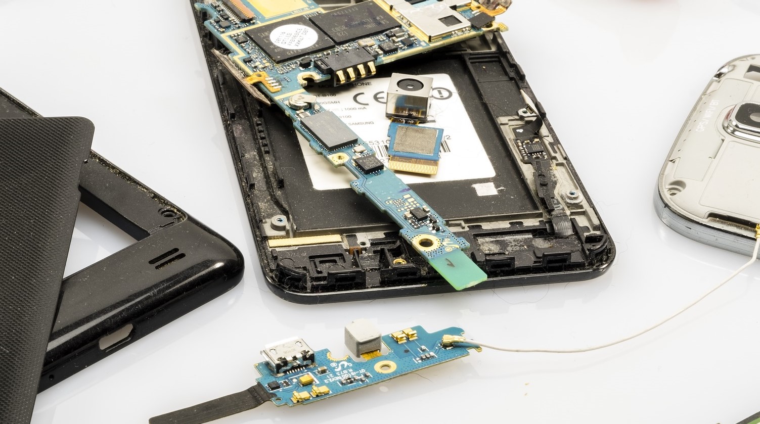
There are many areas in life where accepting mistakes as inevitable is a good thing -- electronics manufacturing is not one of them. The end goal...
Working with small circuit board areas can increase the risk of various PCB defects, tombstoning in particular.
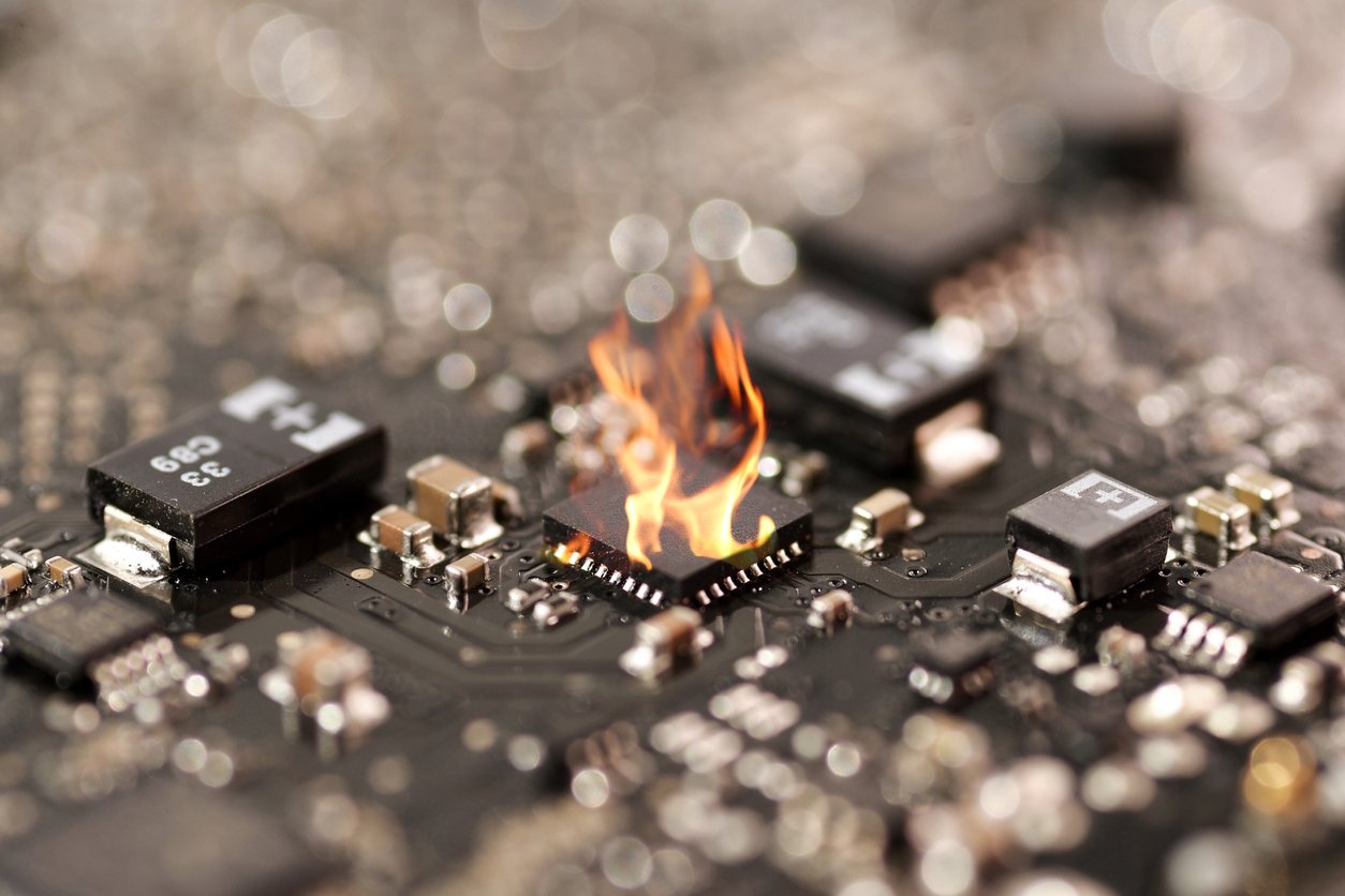
While there are many common printed circuit board defects, one of the most notorious is burnt components. It's also, unfortunately, one of the most...