


 Matric Group
What Is the Cost of a Flying Probe Test?
For many companies, the focus on printed circuit board (PCB) production is on-time-delivery and quality. However, just as important to a product’s...
Testing and inspection are vital parts of electronics contract manufacturing, for obvious reasons. Before that shipment of PCBs arrives on your doorstep, you want to be sure you’re getting what you paid for -- a properly assembled, fully functional circuit board. One of the most important tests your manufacturer can put your boards through to make sure that happens is called burn-in testing, and it could save you a lot of time, money, and trouble.
Let’s look at what burn-in is and how it helps deliver your company more reliable electronics.
Burn-in is the testing of components on a PCB to uncover early failures and establish load capacity.
This is done by running a power supply through the electronics at an elevated temperature, often its maximum-specified capacity. This process is conducted continuously for 48 to 168 hours, with the goal being to snuff out any latent defects triggered by the conditions of the test.
These defects – called infant mortalities – are bad for business. Electronics have a higher failure rate at the beginning of their life cycle, leveling out in the middle and rising again as they reach the end of the life cycle. If a PCB with an infant mortality failure like this were to make its way into military or medical equipment, it could result in a potentially serious failure
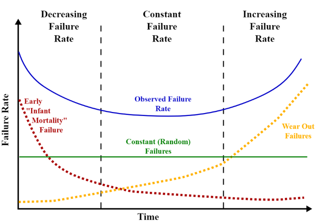 Burn-in testing reduces the number of infant mortality rates by triggering them through this testing, resulting in a more reliable batch of electronics for the OEM, the trade-off being a smaller yield and potentially reduced product lifespan. The data collected through this process can in turn help engineers understand what caused the defects and modify the design to improve product reliability before it even hits burn-in.
If your contract manufacturer is putting your electronics through burn-in testing, be sure that they follow your specified parameters. If the test subjects the electronics to more stress than they’re rated for, it can needlessly deplete their lifespan. If burn-in yields little to no defects after the first 48 hours, testing can be reduced to limit the stress put on good boards given the likelihood of their reliability.
Overall, burn-in testing is one of the more concrete ways an OEM can confirm reliability within its electronics. By eliminating infant mortalities, burn-in reduces the number of defective product that hits the market and extends the average lifetime of products in the process.
Burn-in isn’t a be-all-end-all for testing your electronics. Your electronics contract manufacturer should be able to use additional testing and inspection, such as:
This should ensure that when your electronics are out in the field, they’ll be just as reliable and functional as when they were first manufactured.

For many companies, the focus on printed circuit board (PCB) production is on-time-delivery and quality. However, just as important to a product’s...

Prototyping is just as important to the electronics manufacturing process as designing, engineering, and testing. Ignore it at your own risk.
PCB design is tricky. Depending on how complex your project is -- or how much is at stake if something fails -- you may need top-end testing before...